Introduction
X-ray astronomy is based on the detection of X-rays from celestial sources [1]. The Macau Science Satellite-1B (MSS-1B) is primarily responsible for monitoring solar activity, particularly solar flares, during Solar Cycle 25 [2]. Its main scientific payload is a solar X-ray detector (SXD) that features a wide energy range and a high count rate. The SXD consists of two soft X-ray detection units (SXDUs) with different aperture areas and two identical hard X-ray detection units (HXDUs). These four detection units are integrated into the instrument. This study focuses on the electronic design of the SXDU. The X-ray sensor (XRS) on the GOES satellite provides continuous solar X-ray flux measurements, and the standard X-ray classification of solar flares is based on these measurements [3, 4]. However, the sensor lacks spectral resolution, which limits the physical investigation of coronal emissions in the X-ray spectrum. The Solar Assembly for X-rays (SAX) on MESSENGER consists of a Si-PIN detector with an aperture area of 0.03 mm2. Its energy resolution is 598 eV at 5.9 keV, which isconstrained by Si-PIN noise [5]. The Solar X-ray Spectrometer (SXRS) on the FY-2F mission monitors solar flares above the M1 level with an energy resolution of 185 eV [6]. The HEPP-X onboard the CSES is designed to monitor the solar radiation from a wide field of view [7]. The X-ray spectrometer on MinXSS detects solar X-rays in the 0.8-12 keV range with a time cadence of 10 s [8]. The on-orbit energy resolutions for MinXSS-1 and MinXSS-2 at 5.90 keV are 240 eV for a 4.8 μs peaking time and 168 eV for 1.2 μs, respectively [9]. An improved instrument, known as the Dual-Zone Aperture X-ray Solar Spectrometer, employs a newer version of the SDD and a dedicated aperture design [10]. Its cadence time is set to 9 s. Solar observations are limited to flare levels below M3 due to the detector's saturation limit [11]. These CubeSats and instruments are designed using commercial off-the-shelf electronic devices, and one instrument was previously damaged by a single-event latch-up [12]. The Chandrayaan-2 Solar X-ray Monitor measures the 1-15 keV spectrum from lunar orbit with an energy resolution of 175 eV at 5.9 keV [13]. Its aperture area is limited to 0.367 mm2, making it feasible for detecting flares up to the M5 class. We enhanced the time cadence to 1 s using a dedicated X-ray signal processing design. The peaking times of the shaping amplifiers were optimized to enhance the energy resolution and achieve higher count rates. In particular, two soft X-ray detector units with different aperture areas were integrated to detect solar irradiation, targeting both the quiet Sun and solar flares up to the X-class level.
The primary working principle of the SXD was presented by Shi et al. [14], whereas this study focuses on a detailed description of the SXDU's electronic design and the results of ground calibration. The remainder of this paper is organized as follows. Section 2 presents the basic principles, instrument composition, and specifications. Sections 3–4 describe the design of the X-ray detector module and the analog electronic unit. Section 5 discusses the scientific data types, while Sect. 6 covers spectral performance calibration. Finally, Section 7 presents the conclusions.
Instrument Design
To distinguish the emission lines from those of solar flares, the SXDU is designed with an energy resolution better than 200 eV. The energy range is 1-20 keV. The detector and electronics are identical for both SXDUs. Table 1 lists the specifications.
| Parameter | Specification |
|---|---|
| Energy range (keV) | 1 –20 |
| Energy resolution (eV) | < 200 @ 5.9 keV |
| Aperture area (cm2) | 0.17 and 0.005 |
| Field of view (°) | ±2 |
| Time cadence (s) | 1 |
| Count rate (counts s-1) | ≥ 1×10⁵ |
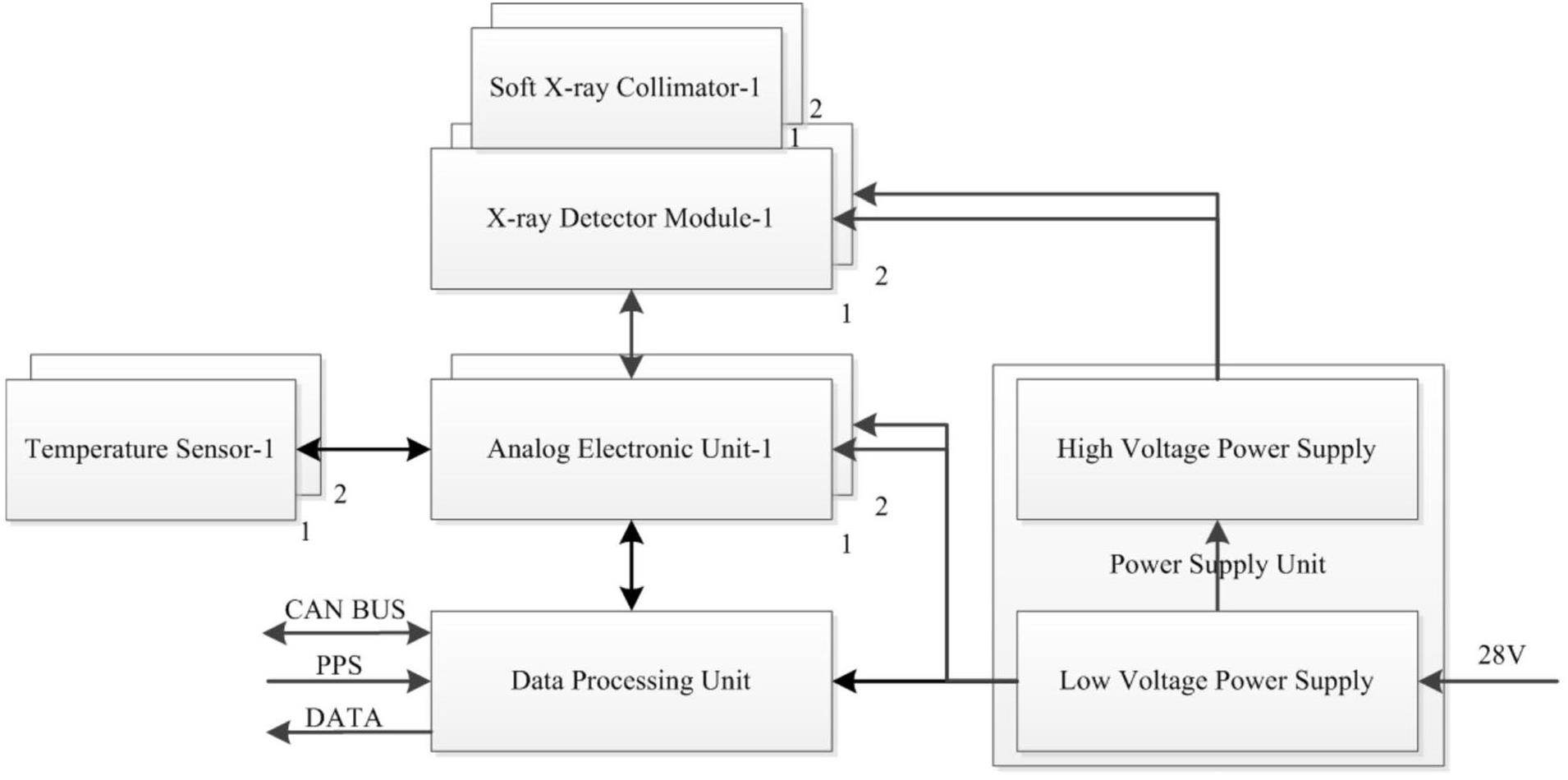
Figure 1 presents a conceptual sketch of the SXDUs. The SXDUs consist of X-ray Detector Modules (XDMs), analog electronic units (AEUs), a data processing unit (DPU), and a power supply unit (PSU). Collimators are positioned in front of the XDMs to restrict the field of view and aperture area. The two XDMs and their associated AEUs share a common DPU and PSU. Detector power is supplied by the low- and high-voltage power supplies within the PSU. The PSU, AEU, and DPU are interconnected via a common bus board for signal transmission and power distribution. Additionally, two temperature sensors are mounted on the AEUs to monitor temperature fluctuations on the analog board.
X-ray Detector Module
SDD detector
Silicon X-ray detectors are widely used in space applications, including silicon drift detectors (SDDs) [15-18], silicon photomultipliers [19, 20], silicon microstrips [21, 22], Si-PIN detectors [23, 24], CCD detectors [25, 26], and APS CMOS imaging sensors [27]. A 500 μm thick SDD is selected as the X-ray sensor. Its unique electrode structure provides an ultralow capacitance, enabling operation at a short peaking time, which increases the count rate. The energy resolution is further improved using a thermoelectric cooler (TEC). The SDD, along with a CMOS charge-sensitive preamplifier, is mounted on the TEC. The detector is positioned behind a thin window composed of a 150 nm silicon nitride film covered with 250 nm aluminum. The two XDMs use the same type of SDD; however, the aperture areas restricted by the collimator are 0.17 cm2 and 0.005 cm2, respectively. A passive graded shield surrounding the detector package protects the detector against space background radiation and fluorescent photons from surrounding materials. Additionally, two 241Am radioactive sources are mounted between the detector plane and collimator in both SXDUs for in-flight calibration and self-verification.
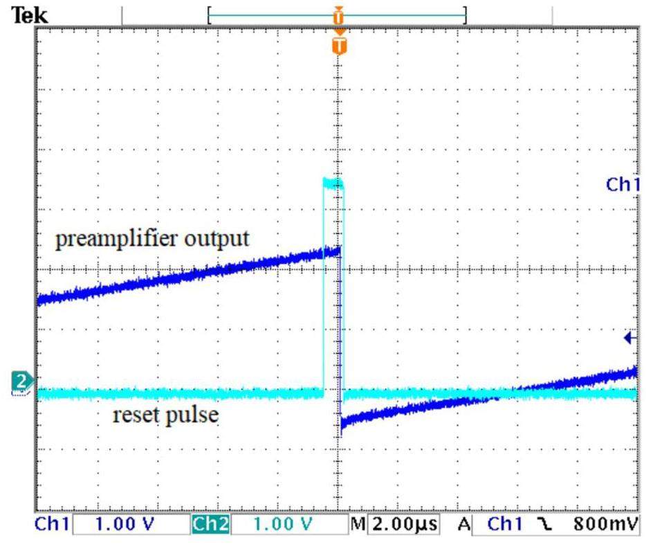
When detector leakage current accumulates in the preamplifier, the ramp output eventually saturates. A reset pulse is applied to restore the detector anode to ground potential, as shown in Fig. 2. The large transient caused by the reset pulse can interfere with signal processing; therefore a window of 10 μs is implemented to eliminate its effects.
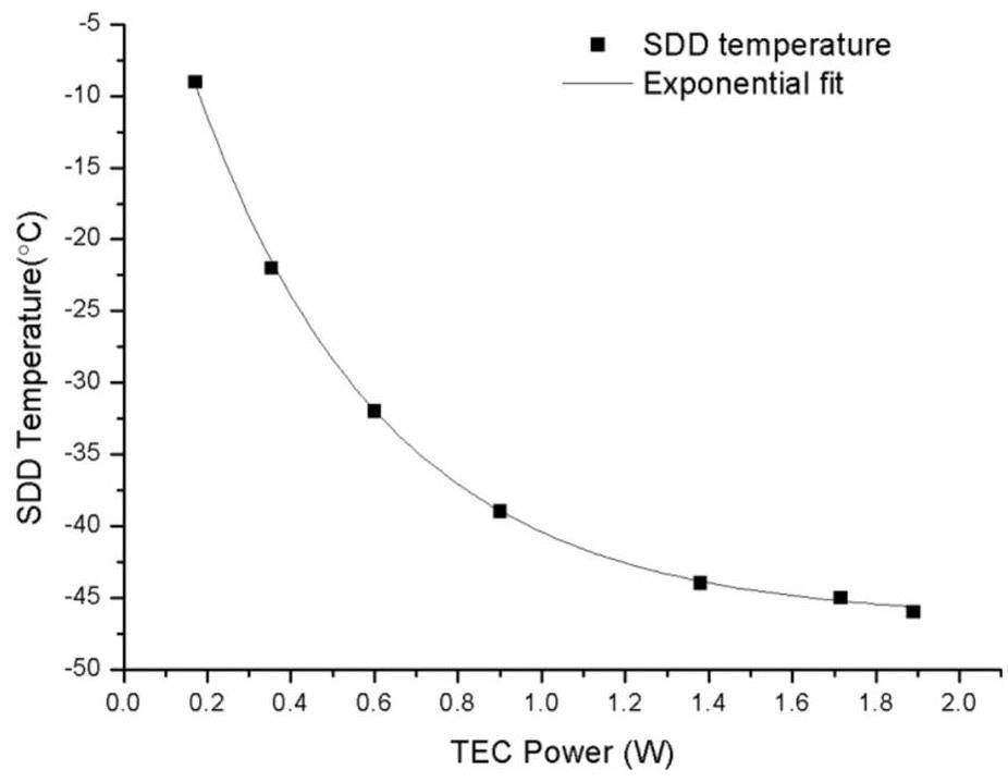
TEC characteristics
The detector leakage current is sensitive to the operating temperature, doubling for every 7 ℃ increase, as described by [28]
Preamplifier reset rate
The preamplifier periodically resets the charge accumulated on the feedback capacitance due to X-ray signals and leakage current:
AEU
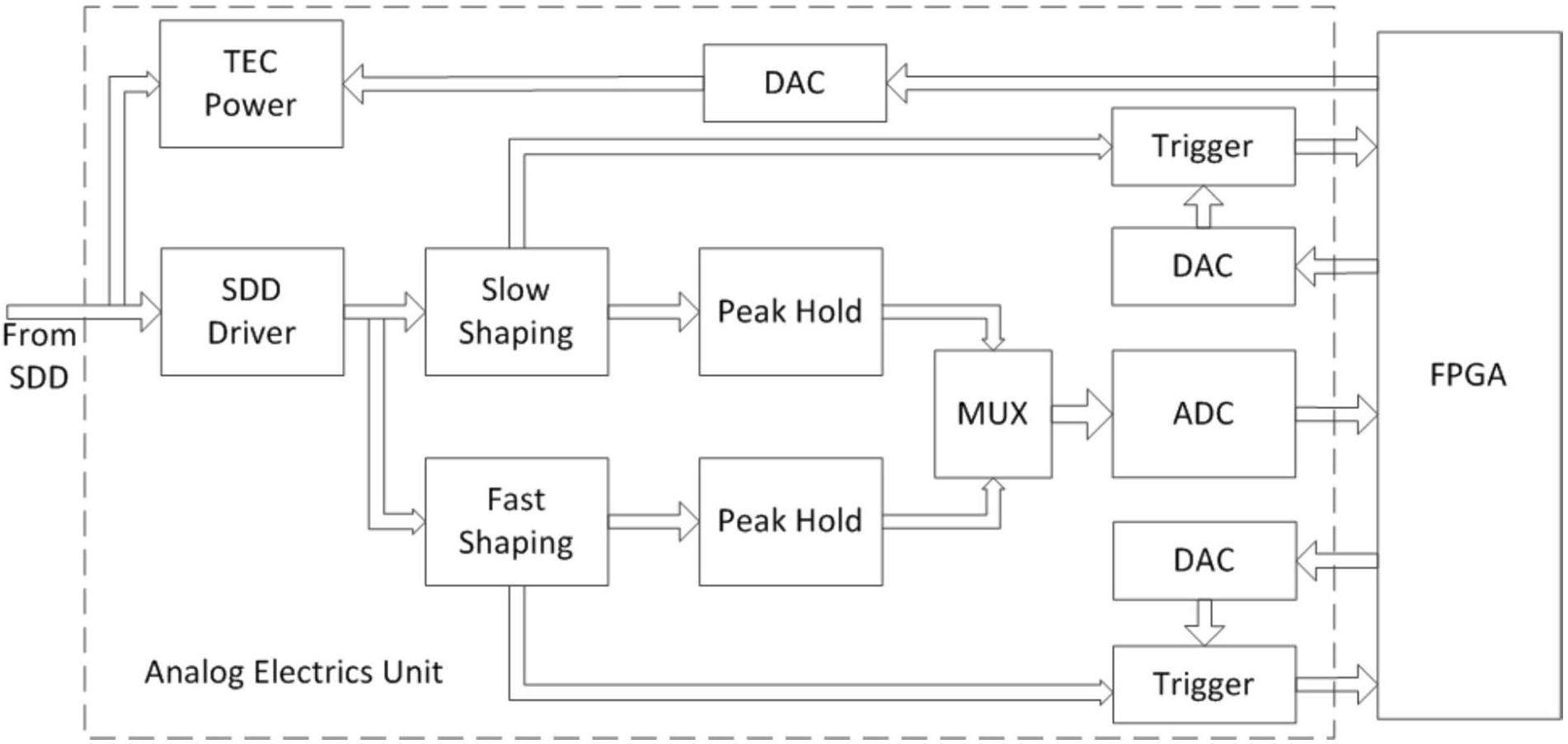
The AEU comprises an SDD preamplifier driver, TEC power driver, and front-end readout electronics, as shown in Fig. 4.
SDD and TEC drivers
The preamplifier driver circuit generates and filters power, sends reset signals to the preamplifier, and buffers and amplifies the preamplifier output to drive the front-end electronics.
The TEC driver reads the temperature diodes inside the SDD package and supplies power to the TEC. The temperature diode is biased using a 160 μA current source. A proportional-integral-derivative (PID) control feedback loop maintains the SDD at the desired temperature, which is set via a digital-to-analog converter (DAC). The TEC power is supplied by a high-efficiency DC-DC converter, with output ripple minimized using an LC-type filter. The voltage and current of the TEC driver, along with the set and measured temperatures, are converted using an ADC. These parameters, together with the ramp-reset rate, are used to assess the operational status of the SDD in orbit.
Shaping amplifier
The preamplifier generates a ramp output composed of small steps. Its output is differentiated to measure the step voltage. The shaping amplifier, designed using two-pole multiple-feedback active low-pass filters [33], as shown in Fig. 5, enhances the signal-to-noise ratio. The amplifiers are optimized to achieve a Bessel phase response, ensuring a constant group delay within the passband. The step response exhibits no overshoot or ringing, which is essential for the performance of the spectrometer. While the rising edge of the shaping output is steep, the voltage decays exponentially back to the baseline. These exponential tails extend many times the duration of the full width at half maximum (FWHM). Pulses that overlap during the extended window pile-up, particularly at high count rates. Reducing the FWHM mitigates pulse pile-up but introduces additional noise.

Two parallel shaping amplifiers with different time constants are designed to serve distinct purposes. The first amplifier is optimized for better timing accuracy, while the second is designed to achieve higher spectral resolution. The shaping amplifiers, with peaking times of 315 ns and 65 ns, are referred to as “slow shaping” and “fast shaping”, respectively. The fast-shaping channel is optimized to improve double-pulse resolution and reduce pile-up; however, it introduces more noise. Consequently, a higher threshold—set by a DAC—is required. In contrast, the slow-shaping channel uses a longer peaking time to extract spectral information. When the amplitude of the slow-shaping channel exceeds the threshold, the peak value is held by the peak holder and digitized by an ADC.
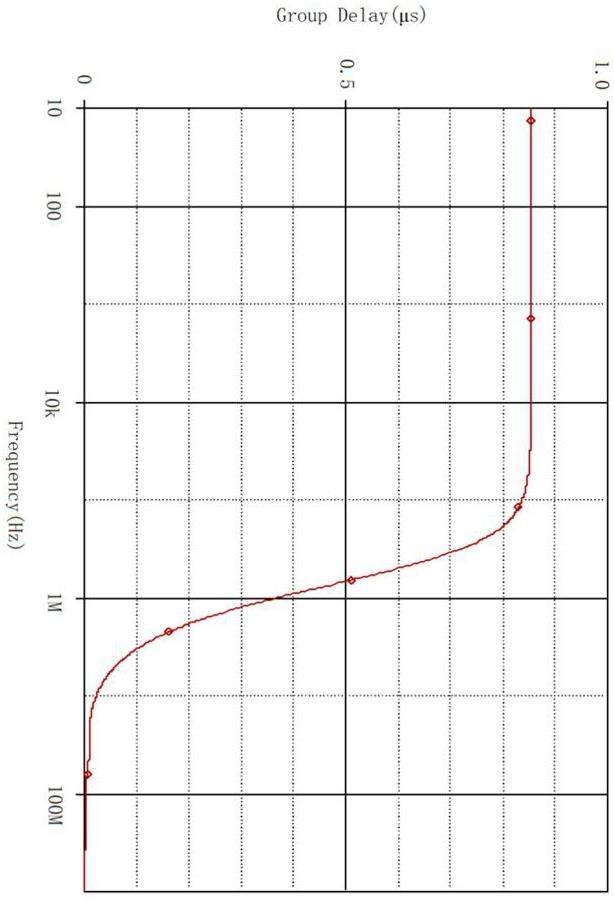
Table 2 lists the design parameters of the slow-shaping channel. The group delay is simulated to be constant in the passband at 853.8 ns, as shown in Fig. 6.
| Parameters | R1 (Ω) | R2 = R3(Ω) | R4 (Ω) | C1 (pF) | C2 (pF) | C3 (pF) | C4 (pF) | R5 = R6 (Ω) | R7 (Ω) | R8 = R9 (Ω) | R10 (Ω) | R11 (Ω) | C5 (pF) | C6 (pF) |
|---|---|---|---|---|---|---|---|---|---|---|---|---|---|---|
| Slow | 200 | 1000 | 51 | 1200 | 220 | 1200 | 10 | 100 | 1500 | 200 | 1300 | 51 | 270 | 680 |
| Fast | 200 | 620 | 10 | 200 | 47 | 47 | 10 | 100 | 2000 | 200 | 2200 | 51 | 32 | 100 |
A pulse generator is connected to the input of the shaping amplifier to simulate the X-ray events. Figure 7 shows the transient response of the slow channel, revealing no overshoot and no ring. The rise time of the slow-shaping amplifier is measured to be 315 ns, the fall time is 945 ns, and the pulse width is less than 2.8 μs.
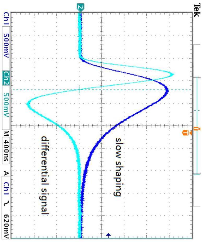
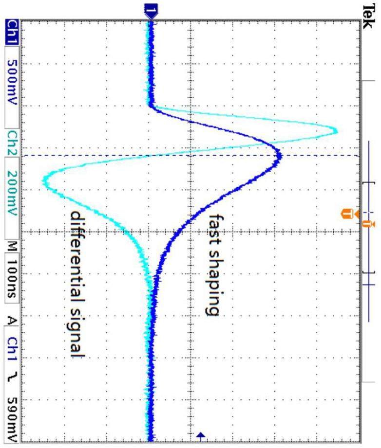
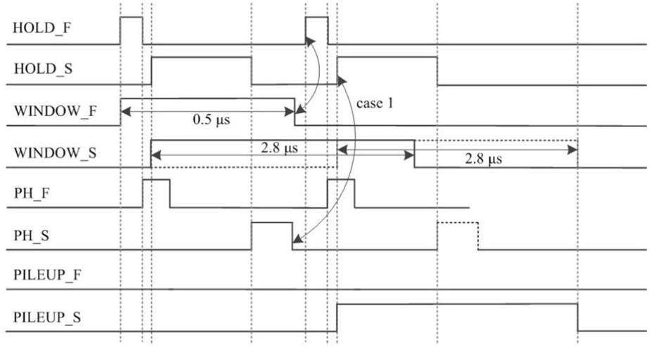
Traditional pile-up detection is performed using a fast/slow-channel approach [34]. It cannot distinguish pulses that overlap in the fast channel. The differential of the shaping amplifier generates a bipolar output. As Fig. 8 shows, the pulse width of the differential signal is significantly smaller than that of the shaping amplifier. Therefore, the differential signals of the fast channel are selected for pile-up rejection.
The time interval of an X-ray photon can be described by an exponential distribution.
Peak-hold circuit
The rise time of the SDD output is a function of the incident position [35]. The peaking time of the slow channel is significantly longer than the variation in the rise time, with a maximum of 30 ns. Therefore, the amplitude of the slow-channel amplitude does not depend on the event position. The flat-top duration of the fast channel is shorter than the rise time, leading to pulse height loss due to the ballistic deficit. As a result, events originating far from the center could be rejected by comparing the fast and slow amplitudes. Both peak values are sampled for space-background rejection.
The diagram of the peak-hold circuit is shown in Fig. 9. A CMOS analog switch is inserted between the shaping amplifier and the hold-capacitor stage. When a pulse peak is detected, the peak value is held in the capacitor by turning off the switch until it is read out by a 16-bit ADC. Only the 12 most significant bits are stored. The charge on the capacitor is reset by turning on the switch. The peak value from the capacitor is buffered by a unit-gain operational amplifier with a low input-bias current. Additionally, low-leakage, low-dielectric absorption capacitors are essential. The peak value of the fast-shaping amplitude is obtained in the same manner, with both the fast and slow peak-hold circuits sharing a common ADC. Figure 10 shows the input waveform of the ADC. A CMOS analog switch is used to select a single channel. The switch features an extremely high switching speed and ensures break-before-make switching. The charge injection is less than 2 pC, which is crucial for high-precision peak-height capture.
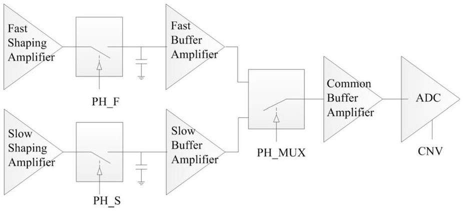
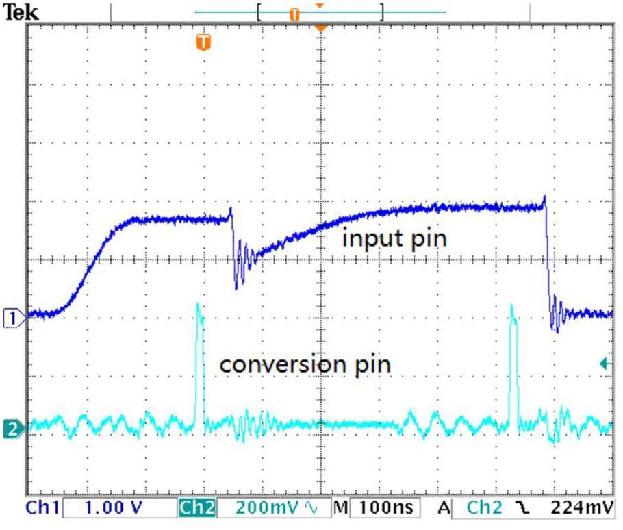
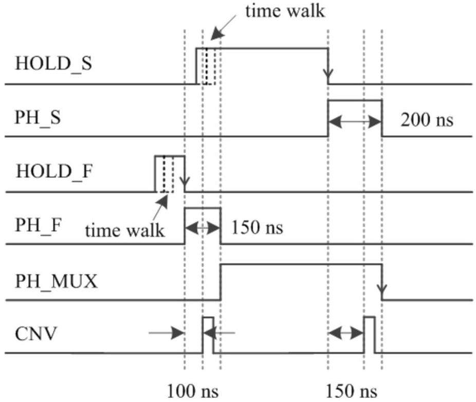
Figure 11 shows the timing of the switches in the peak-hold circuit. The durations of the peak-hold signals “PH_F” and “PH_S” for the fast and slow channels are 150 ns and 200 ns, respectively. The ADC starts the conversion signal, “CNV”, for the two channels with delays of 100 ns and 150 ns, respectively. At the end of each peak-hold signal, the switch changes its state. It is important to note that, in some cases, “PH_F” may be absent, as the fast channel threshold is higher. As a result, the assertion of “PH_MUX” is controlled by both “HOLD_S” and “PH_F.” Here, “HOLD_S” is the “HOLD” signal of the slow channel, while “HOLD_F” corresponds to that of the fast channel. At the rising edge of “HOLD_S”, if “PH_F” is high, then “PH_MUX” is asserted at the falling edge of “PH_F”; otherwise, “PH_MUX” is asserted immediately.
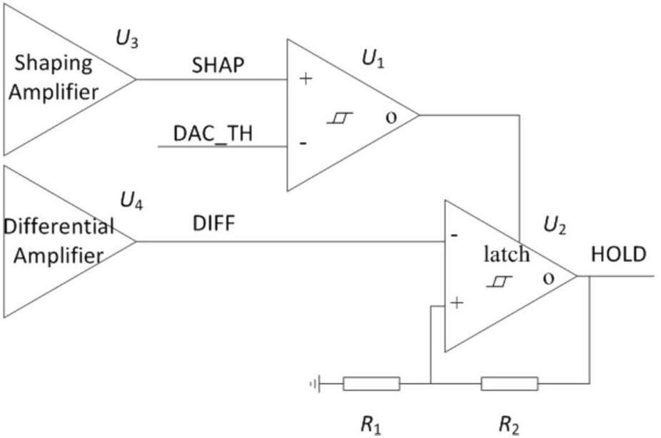
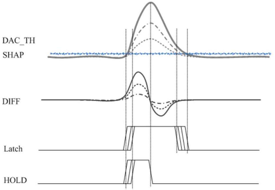
The “HOLD” signal is generated by connecting the differentiating amplifier output to a comparator with hysteresis. “HOLD_S” and “HOLD_F” are generated in the same approach, as shown in Fig. 12 and 13. The comparator U2 output, known as “HOLD,”, switches to high for input voltages greater than VHI and does not switch to low until the input voltage is less than VLO (i.e., at the zero crossing).
Pile-up rejection
If the two pulses are too close in time, the height of the second pulse can be affected. Errors in the measured pulse height may distort the spectrum. The overlapping pulse in the slow channel was identified using the differential signal of the fast channel, as described earlier. To obtain a clean spectrum, all overlapping pulses are rejected. The analog shaper exhibits an infinite impulse response. Even when the tail drops rapidly toward the baseline, a small contribution remains [36]. The dead-time window widths, “WINDOW_S” and “WINDOW_F”, for the slow and fast channels, are 2.8 μs and 0.5 μs, respectively, as shown in Fig. 14. If an event occurs during the dead time, the dead time is extended, which reduces throughput. Therefore, the dead time can be described using a paralyzable model, as shown in Fig. 15 [37].
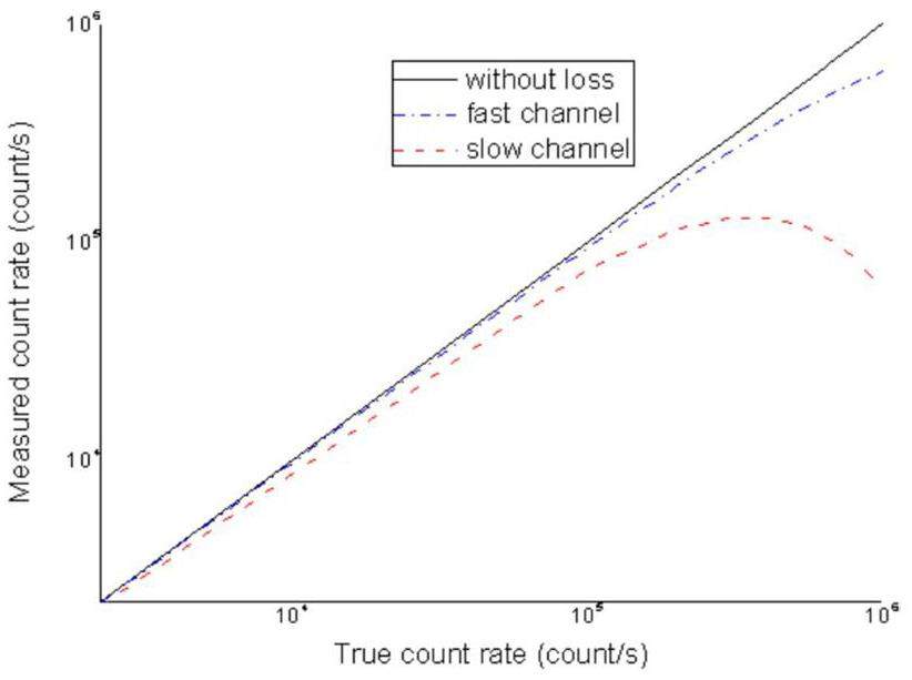
The fraction without loss is
Operating Mode Design
The SXDU generates three types of observation modes, in addition to the default standby mode.
In standby mode, after being powered on, the SXDU operates with the XDMs and AEUs powered off. The selected detector channel is powered by a command. Following initialization, the SXDU switches to the selected observation mode.
The baseline noise observation mode is primarily used to enable detailed monitoring of detector performance, particularly the evaluation of noise after radiation exposure. The signal amplitude is sampled every 10 ms, regardless of the incident events.
In the spectrometer histogram observation mode, each valid pulse height is stored in its respective channel to obtain a spectrum histogram with 2048 channels. The histogram depth is 3 bytes, generating 6 KB of histogram data every second.
The photonlist observation mode samples the pulse heights in both channels sequentially using a 16-bit ADC. Data for each event consists of the detector number, trigger mode, time stamp, and pulse height data. Each transfer frame consists of 512 events, and the data capacity is limited by the interface clock to a maximum of 40 frames per second.
Spectral Performance
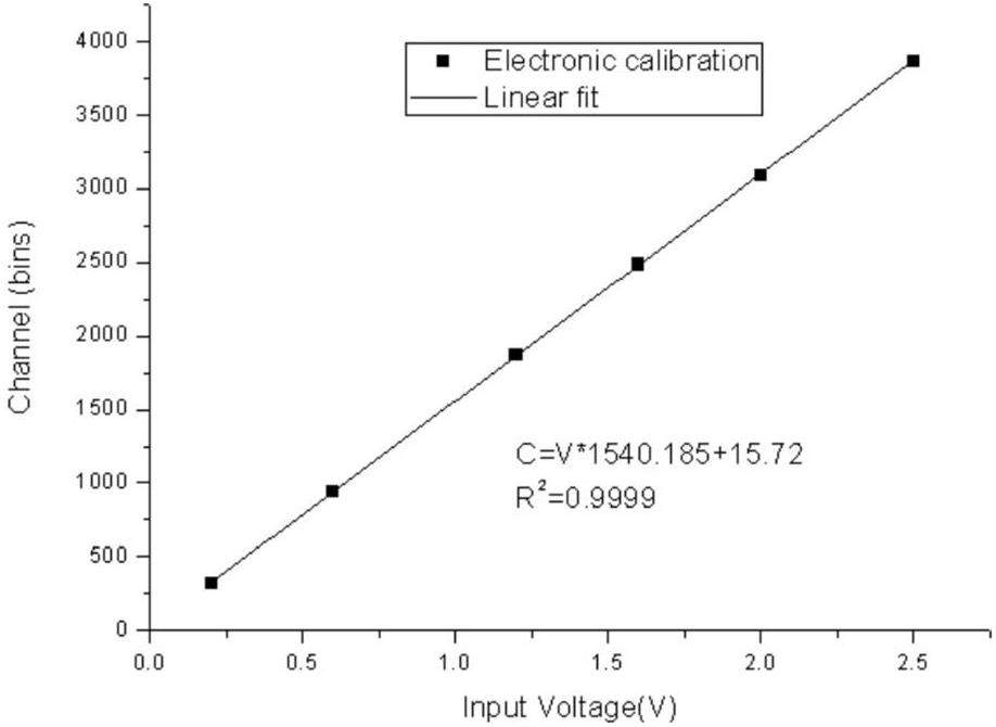
It is desirable to obtain a linear energy response in solar spectroscopy. Before the X-ray sources are applied, a step signal generator, instead of an X-ray detector, is connected to the front-end readout electronics. The step voltage is attenuated 80 times using a small resistor to reject noise. The sampled peak values are scaled linearly with the input voltage, as shown in Fig. 16.
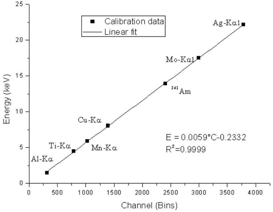
A miniature X-ray tube with a W target is used to obtain the fluorescence lines from aluminum (1.49 keV), titanium (4.51 keV), manganese (5.90 keV), copper (8.05 keV), molybdenum (17.48 keV) and silver (22.17 keV). The emission line at approximately 13.94 keV from the 241Am radioactive source is included. Spectral performance is evaluated using the Kα1 line centroid and width. During calibration, the detector temperature is maintained at -30 ℃.
Figure 17 shows the linear calibration using X-ray sources. The gain and offset are obtained by linear fitting. The gain is 5.9 eV/channel when operated in the photonlist observation mode. The offset is approximately -233 eV with an error of 42 eV. The upper and lower limits of the energy range are 23.39 keV and 0.7 keV, respectively.
The energy resolution calibrated using various X-ray sources are listed in Table 3. The Kα line is the sum of the two lines. The Kα1 lines for 241Am, Mo, and Ag are shown.
| X-ray Source | Energy (keV) | FWHM(eV) | Error(eV) |
|---|---|---|---|
| Al-Kα | 1.49 | 96.97 | 1.10 |
| Ti-Kα | 4.51 | 127.16 | 0.44 |
| Mn-Kα | 5.90 | 138.00 | 0.42 |
| Cu-Kα | 8.05 | 165.68 | 1.98 |
| 241Am | 13.94 | 221.62 | 4.05 |
| Mo-Kα1 | 17.478 | 238.45 | 20.85 |
| Ag-Kα1 | 22.162 | 262.28 | 17.78 |
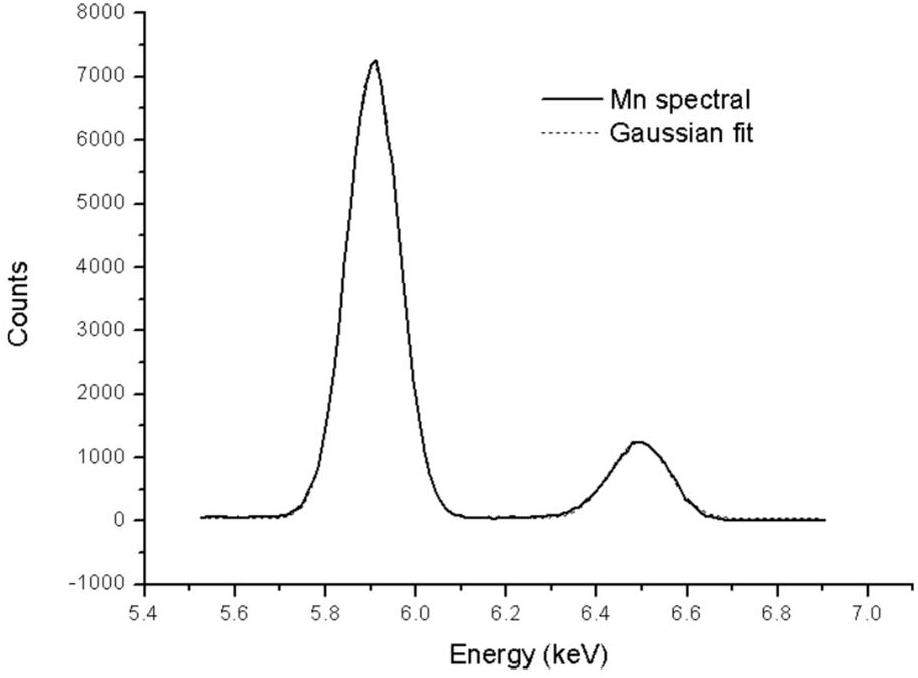
Figure 18 shows the spot spectrum of the Mn fluorescence lines. The 5.90-and 6.49 keV line complexes are clearly detected. The spectral lines are fitted with a Gaussian function to obtain the peak channel centroid and FWHM. The measured energy resolution is 138 eV at 5.90 keV, which is markedly better than the requirement of 200 eV. Compared to the instruments listed in Table 4, this study demonstrates better energy resolution with a lower peaking time, indicating a higher solar flare level and better spectral resolution.
| Instrument Sensor | SXRS [6] SDD | HEPP-X [7] SDD | SXM [13] SDD | MinXSS [8] SDD | This study SDD |
|---|---|---|---|---|---|
| Sensor area | 7 mm2 | 7 mm2 | 30 mm2 | 25 mm2 | 25 mm2 |
| Energy range | 1.5-24.8 keV | 0.9-35 keV | 1-15 keV | 0.5-30 keV | 0.7-23.97 keV |
| Field of view | ± 26° | ±30° ×±50° | ±40° | ±2° | ±2° |
| Energy resolution | 185 eV @ 5.88 keV | 175 eV @ 5.90 keV | 175 eV @ 5.90 keV | 168 eV @ 5.90 keV | 138 eV @ 5.90 keV |
| Peaking time | / | / | 1.0 μs | 1.2 μs | 315 ns |
| Count rate | / | 10 kcps | 80 kcps | 255 kcps | 100 kcps |
| Cadence | 2.05 s | / | 1 s | 10 s | 1 s |
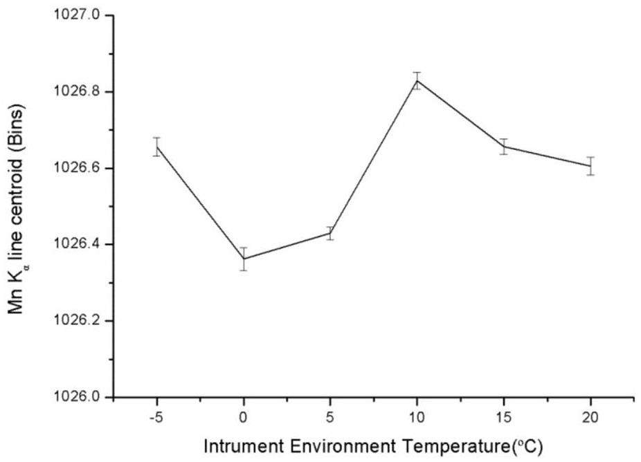
As shown in Fig. 19, the centroid drift in the temperature range of -5 ℃ to 20 ℃ is less than 0.6 ADC bin, which is calibrated to approximately 3.6 eV. These results demonstrate the low noise and high accuracy of the electronic read-out design of solar X-ray spectrometers.
Conclusion
This study presents the design and ground calibration of a solar soft X-ray detection unit on the MSS-1B satellite. The core component of the X-ray module is a silicon drift detector, chosen for its excellent energy resolution. The detector is nominally cooled to -30 ℃ using a TEC. The preamplifier output voltage is further processed by two parallel shaping amplifiers with peaking times of 315 ns and 65 ns. The slow-shaping channel, optimized for spectroscopy, operates with a higher peaking time, while the fast channel is used for pile-up rejection. The linearity response was validated using an electronic signal generator and various X-ray sources. The measured energy resolution is 138 eV at 5.90 keV, with a centroid drift of less than 3.5 eV over a temperature range of -5 ℃ to 20 ℃. Compared with other on-orbit solar X-ray instruments, this study demonstrates improved energy resolution with a lower peaking time, enabling higher sensitivity to solar flare levels and better spectral resolution. These results highlight the low-noise, high-accuracy read-out electronics design of the solar X-ray spectrometer.
X-ray tomography of hidden matter in the Universe
. Sci. Bull. 86, 3120-3123 (2023). https://doi.org/10.1016/j.scib.2023.11.033A novel geomagnetic satellite constellation: science and applications
. Earth Planet Phys. 7, 4-21 (2023). https://doi.org/10.26464/epp2023019Report on GOES SXI/XRS calibration effort
. In:Next generation X-ray sensor (XRS) for GOES-R Satellite Series
. In:Solar flare element abundances from the Solar Assembly for X-Rays (SAX) on MESSENGER
. ApJ. 803, 67 (2015). https://doi.org/10.1088/0004-637X/803/2/67Pre-flight calibration and the first results for the solar X ray spectrometer (SXRS) onboard FY-2F satellite
. Chin. J. Geophys. (in Chinese). 57, 3812-3821 (2014). https://doi.org/10.6038/cjg20141135The high-energy particle package onboard CSES
. Radiat. Detect. Technol. Methods. 3, 1-11 (2019). https://doi.org/10.1007/s41605-019-0101-7The instruments and capabilities of the miniature X-ray solar spectrometer (MinXSS) cubeSats
. Sol. Phys. 293, 21 (2018). https://doi.org/10.1007/s11207-018-1243-3MinXSS-2 cubesat mission overview: improvements from the successful MinXSS-1 mission
. Adv. Space Res. 66, 3-9 (2020). https://doi.org/10.1016/j.asr.2019.02.011Soft X-ray observations of quiescent solar active regions using the novel dual-zone aperture X-ray solar spectrometer
. ApJ. 904, 20 (2020). https://doi.org/10.3847/1538-4357/abba2aFirst results for solar soft X-ray irradiance measurements from the third generation miniature X-ray solar spectrometer
. ApJ 956, 94 (2023). https://doi.org/10.3847/1538-4357/acef13Achievements and lessons learned from successful small satellite missions for space weather-oriented research
. Space Weather. 20,Solar X-ray monitor on board the Chandrayaan-2 orbiter: in-flight performance and science prospects
. Sol. Phys. 295, 139 (2020). https://doi.org/10.1007/s11207-020-01712-1Design of the solar X-ray detector for the macau science satellite-1B
. Earth Planet Phys. 7, 125-130 (2023). https://doi.org/10.26464/epp2023018High resolution solar soft X-ray spectrometer
. Chin. Phys. C. 36, 146-150 (2012). https://doi.org/10.1088/1674-1137/36/2/008Next generation Space Environment Monitor (SEM) for FY-2 satellite series.(in Chinese)
. Chin. J. Geophys. 56, 1-11 (2013) https://doi.org/10.6038/cjg20130101Data processing for the Active Particle-induced X-ray Spectrometer and initial scientific results from Chang'e-3 mission
. Res. Astron. Astrophys. 14, 1595 (2014) https://doi.org/10.1088/1674-4527/14/12/008Readout electronics for a high resolution soft X-ray spectrometer based on silicon drift detector
. Nucl. Sci. Tech. 28, 14 (2016). https://doi.org/10.1007/s41365-016-0160-0Compact CubeSat Gamma-ray detector for GRID mission
. Nucl. Sci. Tech. 32, 99 (2021). https://doi.org/10.1007/s41365-021-00937-4Performance analysis of LYSO–SiPM detection module for X-ray communication during spacecraft reentry blackout
. Nucl. Instrum. Meth. A 1013,Characterization of silicon microstrip sensors for space astronomy
. Nucl. Sci. Tech. 31, 97 (2020). https://doi.org/10.1007/s41365-020-00811-9Simulation of DAMPE silicon microstrip detectors in the Allpix2 framework
. Nucl. Instrum. Meth. A 1057,In-orbit performance of ME onboard Insight-HXMT in the first 5 years
. Radiat. Detect. Technol. Methods 7, 15-24 (2023). https://doi.org/10.1007/s41605-023-00395-zA cross-type imaging electron spectrometer
. Sci. China Tech. Sci. 66, 641-653 (2023). https://doi.org/10.1007/s11431-022-2103-7Design and simulation of Soft X-Ray imager on SMILE satellite
(in Chinese). Chin. J. Geophys. 61, 4348-4355 (2018). https://doi.org/10.6038/cjg2018L0734The Low Energy X-ray telescope (LE) onboard the Insight-HXMT astronomy satellite
. Sci. China Phys. Mech. Astron. 63,First Wide Field-of-view X-Ray Observations by a Lobster-eye Focusing Telescope in Orbit
. Astrophys. J. Lett. 941,Effect on characteristic of silicon drift detector by electron exposure
(in Chinese). J. Beijing Univ. Aeronaut. Astronaut. 39, 235-238, (2013) https://bhxb.buaa.edu.cn/bhzk/cn/article/Y2013/I2/235.The effect of the displacement damage on the charge collection efficiency in silicon drift detectors for the LOFT satellite
. J. Instrum. 10,Radiation effects on Silicon Drift Detector based X-ray spectrometer on-board Chandrayaan-2 mission
. J. Instrum. 10,Investigation of radiation damage due to particle irradiation on Silicon Drift Detector for Chandrayaan-2 mission
. J. Instrum. 15,NICER instrument detector subsystem: description and performance
. In:Optimal pulse processing, pile-up decomposition, and applications of silicon drift detectors at LCLS
. IEEE Trans. Nucl. Sci. 64, 2854-2868 (2017). https://doi.org/10.1109/TNS.2017.2762281Characterization of the silicon drift detector for NICER instrument
. In:Dead time correction in the DP5 digital pulse processor
. In:Radiation detector deadtime and pile up: A review of the status of science
. Nucl. Eng. Technol. 50, 1006-1016 (2008). https://doi.org/10.1016/j.net.2018.06.014The authors declare that they have no competing interests.

