Introduction
Imaging detection systems using CMOS image sensors(CISs) have high application prospects in radiation environments owing to their advantages, such as low power consumption, improved electro-optical performance, and high tolerance to total ionizing dose (TID) effects [1-5]. Several previous studies have investigated the radiation effects of CISs, showing that they are particularly susceptible to displacement damage dose (DDD) effects. However, effective methods for radiation hardening have not yet been proposed [6-9]. Consequently, evaluating and estimating the DDD effects on CISs has become essential.
For Si-based devices, the concept of equivalent DDD, introduced by the US Naval Research Laboratory [10], has been utilized to assess the degradation caused by displacement damage from various particles, such as neutrons, protons, and heavy ions. The DDD effect on the mean dark signal of CISs with different structures under neutron or proton irradiation is consistent with the theory of equivalent DDD, as demonstrated by Virmontois and Goiffon [11, 12]. In addition to the mean dark signal, dark signal non-uniformity (DSNU) and dark signal distribution are crucial parameters for evaluating CIS performance, considering that CISs operate as an array of photodiodes. Analyzing the mean dark signal alone is insufficient for a comprehensive assessment of the impact of displacement damage on CIS. Unfortunately, the DDD effect on DSNU and dark signal distribution has not yet been elucidated.
Neutron irradiation experiments are commonly employed to investigate equivalent DDD effects induced by protons, heavy ions, or mixed particles [13, 14]. Typically, the irradiation fluence is converted to an equivalent 1-MeV neutron fluence for standardization. In previous assessments of DDD effects on CIS, DDD has been considered, but the influence of neutron energy is usually overlooked. The impact of neutron energy on the DDD effect in dark signals, especially on DSNU, dark signal distribution, and hot pixels, should be investigated to effectively assess the overall effect of DDD on CIS performance.
This study investigated the DDD effect on the mean dark signal, DSNU, dark signal distribution, and hot pixels induced by back-streaming white neutrons (Back-n) at the China Spallation Neutron Source (CSNS) and Xi’an Pulsed Reactor (XAPR). Parameter degradation was evaluated via an analysis that employed the theory of equivalent DDD. To assess the energy distribution of the primary knock-on atoms (PKAs) and non-ionizing energy loss (NIEL) induced in Si by 1-MeV wide-spectrum neutrons at CSNS back-n and XPAR with an equivalent neutron energy of 1 MeV, the open-source package Geant4 was employed for calculations. Research findings were analyzed by combining the results from both experimental and simulation approaches.
Experimental Details
Samples
Two types of CISs (CIS1 and CIS2) were used in our experiments. The cross sections of the pixel structures of CIS1 and CIS2 are presented in Fig.1. CIS1 is a frontside illuminated scientific CIS comprising 11 μ m-pitch 2048 × 2048-pixel arrays. The active image size is 22.5 mm × 22.5 mm, and it is packaged in a 115-pin micro pin grid array (μPGA) package. The temporal noise is approximately 1.47e-, and the dynamic range exceeds 96 dB in high dynamic range mode. The power consumption of the image sensor operating at full speed is less than 600 mW. CIS2 is a backside-illuminated scientific CIS comprising 6.5 μ m-pitch 2048 × 2048-pixel arrays. The active image size is 13.3 mm × 13.3 mm, and it is packaged in a 153-pin μPGA package. The temporal noise is almost 1.20e- with two-correlated multiple sampling (CMS) operations, and the dynamic range exceeds 90 dB. Both CIS circuits were fabricated using a 0.18-μm commercial CIS process. The CISs employ a P+/N/P sandwich structure, known as a pinned photodiode to accumulate charges during integration. When the transfer gate is open, charges collected in the depletion region (also referred to as the space charge region, SCR) of the CIS pixel are transferred to the floating diode and subsequently read. Shallow trench isolation surrounds the photodiode to minimize crosstalk. Compared with traditional photodiodes, such as PN diodes or PIN diodes, a CIS consists of millions of pixels that demonstrate unique statistical properties, rendering it suitable for analyzing the DDD effect.

Experimental Setup
Neutron irradiation experiments were conducted at XAPR and CSNS back-n facilities. In our experiment, we used four CIS samples: CIS1-#1, CIS1-#2, CIS1-#3, and CIS1-#4. CIS1-#1 was exposed to a 1-MeV neutron equivalent fluences of 1 × 10¹¹ n/cm2 and 2 × 10¹¹ n/cm2 at XAPR. CIS1-#2 was exposed to CSNS back-n with fluences of 5 × 10⁹ n/cm2, 1 × 10¹⁰ n/cm2, 3 × 10¹⁰ n/cm2, 6.5 × 10¹⁰ n/cm2, and 1 × 10¹¹ n/cm2. CIS1-#3 was exposed to a 1-MeV neutron equivalent fluence of 1×10¹¹ at the XAPR. CIS1-#4 was exposed to CSNS back-n with fluence of 1 × 10¹⁰ n/cm2, 3 × 10¹⁰ n/cm2, 5 × 10¹⁰ n/cm2, 1 × 10¹¹ n/cm2, and 2 × 10¹¹ n/cm2. All CISs were unbiased during irradiation. The energy of XAPR neutron irradiation ranges from meV to 20 MeV, while that of the CSNS back-n neutron irradiation ranges from eV to 200 MeV [15-19]. The accuracy of the XAPR neutron irradiation fluence was within 10%, and that of the CSNS back-n irradiation fluence was within 5%. The mean dark signal, DSNU, and dark signal distribution were measured after neutron irradiation. The ambient laboratory temperature was controlled using an air conditioner and maintained at approximately 25 ℃. Images were captured until the output of the test system was stable to ensure that the measured uncertainty was less than 1%. The parameters were then calculated using a program developed by our research team.
Simulation details
To investigate the disparity in radiation effects on the CIS induced by neutrons at CSNS back-n and XAPR, Monte Carlo simulations were conducted using the open-source package Geant4 version 11.0 [20-22]. The sensitive region of the CIS comprises Si with a thickness not exceeding 5 μm. To enhance simulation efficiency, a simplified geometry was employed to simulate the DDD effect on the CIS. The geometry was simplified to a single Si box with dimensions of 1 cm × 1 cm × 2 mm, representing a ’quasi-infinite’ homogeneous medium. Incident particles were directed toward the center of the Si box, as shown in Fig. 2(a). The cross-section of the neutron interaction with Si used in our Geant4 simulations is shown in Fig. 2(b). The energy spectrum of PKAs resulting from neutron interactions was computed.
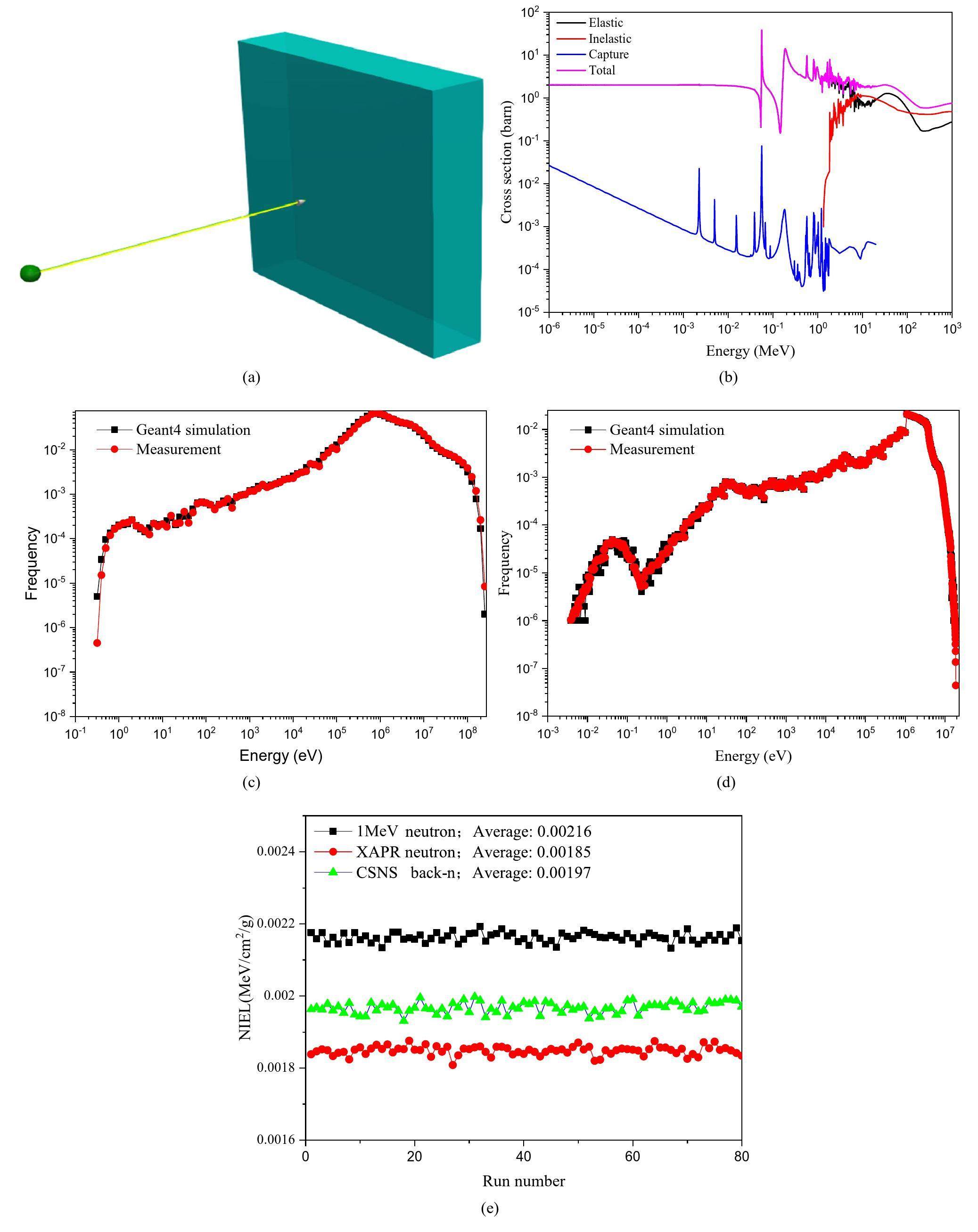
The DDD is then calculated using the NIEL and irradiation fluence [23].
Results and analysis
Mean dark signal
The mean dark signal represents the average value of the dark signal for each pixel of the CIS array, without any charge injected by light, particles, or electrical means. This parameter is significant for evaluating CIS performance. The mean dark signal is expressed as follows [27]:
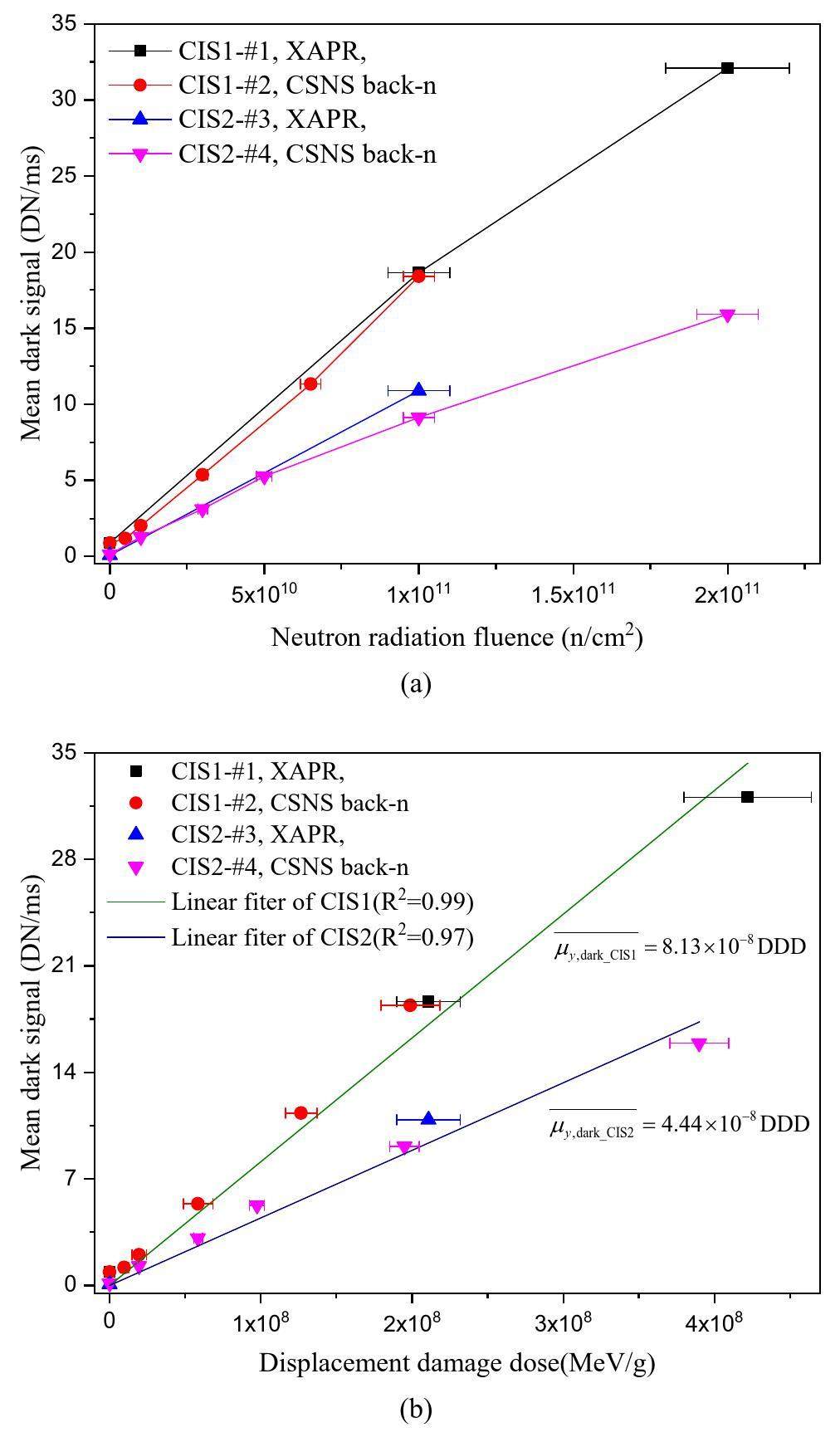
In our experimental setup, the fluence of the XAPR neutron was equivalent to that of a 1-MeV neutron. Therefore, the NIEL of a 1-MeV neutron was employed to represent the NIEL of the XAPR neutron. However, the NIEL of a 1-MeV neutron is not greater than 10% of that of the CSNS back-n, which is similar to the accuracy of the irradiation fluence. The radiation damage induced by the XAPR and CSNS back-n neutrons is almost similar. As shown in Fig. 3(a), the XAPR neutron causes damage similar to that of the CSNS back-n at an equivalent irradiation fluence, confirming our observations. Figure 3(b) shows the relationship between the mean dark signal and DDD following XAPR neutron and CSNS back-n irradiation. Data uncertainties, including the accuracy of the irradiation fluence and simulation uncertainties, are presented. As shown in Fig. 3(b), the increase in the mean dark signal is proportional to the DDD. This result is consistent with the findings of Goiffon and Srour [12, 24]. The goodness-of-fit of the linear regression model was calculated, yielding a value of approximately 0.991 for CIS1 and 0.986 for CIS2. Thus, the relationship between the mean dark signal and DDD can be expressed as
Dark signal non-uniformity
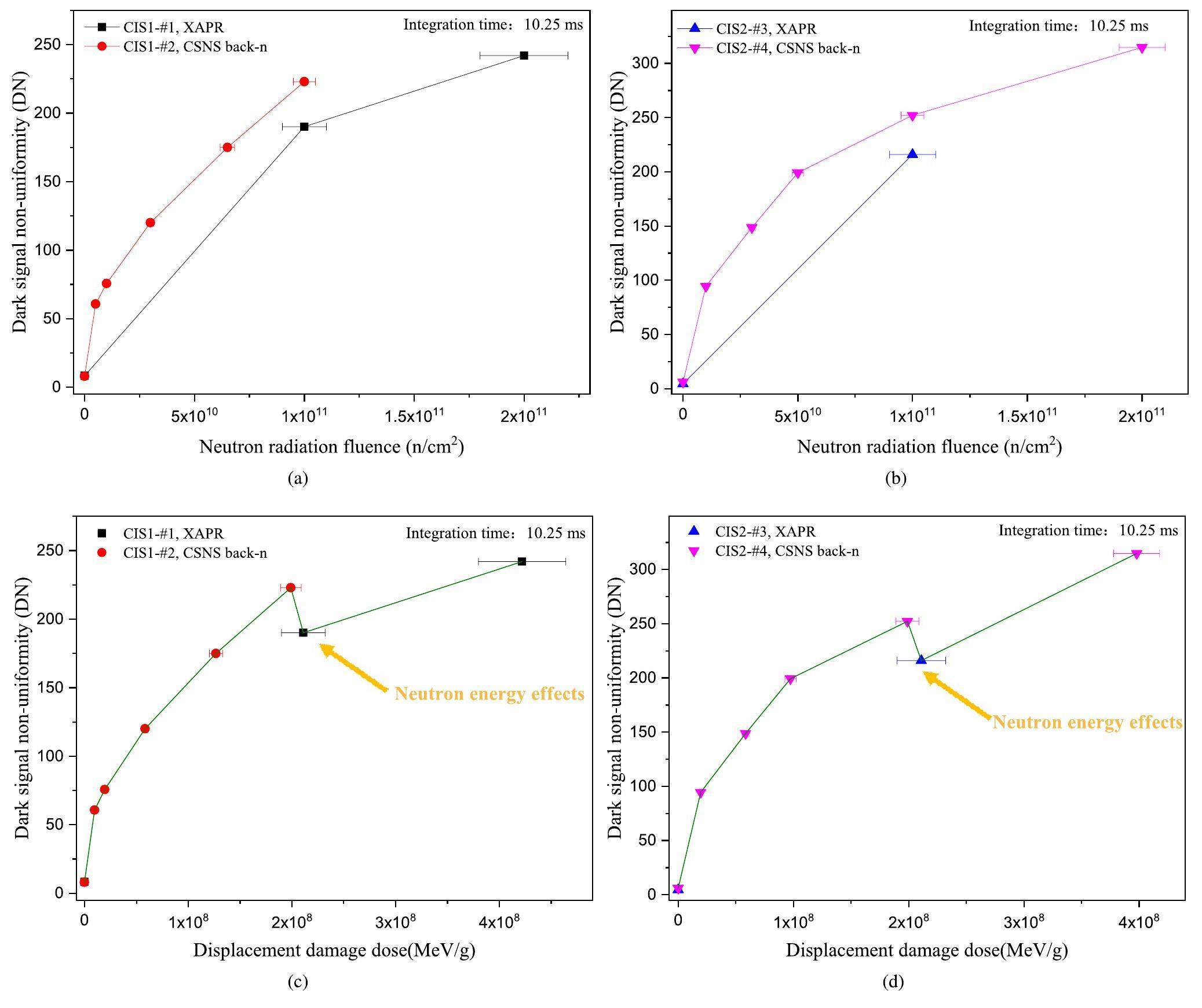
The DSNU is a measure of the non-uniformity of the dark signal within CIS arrays. This is defined as follows [27]:
Dark signal distribution
Dark signal distribution refers to the variation in the dark signal among individual pixels within CIS arrays in the absence of external light, particles, or electrical inputs. Figure 5(a)–(d) show the dark signal distributions of the CIS after exposure to CSNS back-n and XAPR neutron irradiation. The irradiation fluence for both cases is approximately 1 × 10¹¹ n/cm2 (for the XAPR neutron, the irradiation fluence represents a 1-MeV neutron equivalent fluence). As shown in Fig. 5(a)–(d), noticeable differences can be observed in the dark signal distributions resulting from CSNS back-n and XAPR neutron irradiation. The dark signal distribution can be analyzed in three distinct regions. In region I, the dark signal of the CIS exhibits minimal variation after irradiation by the CSNS back-n and XAPR neutrons. This region primarily comprises pixels that are largely unaffected by neutron irradiation, with minor differences likely attributable to variations in production technology. In region II, the number of pixels damaged by XAPR neutron irradiation exceeded those damaged by the CSNS back-n. In region III, the number of pixels damaged by CSNS back-n irradiation exceeded that damaged by XAPR neutron irradiation.
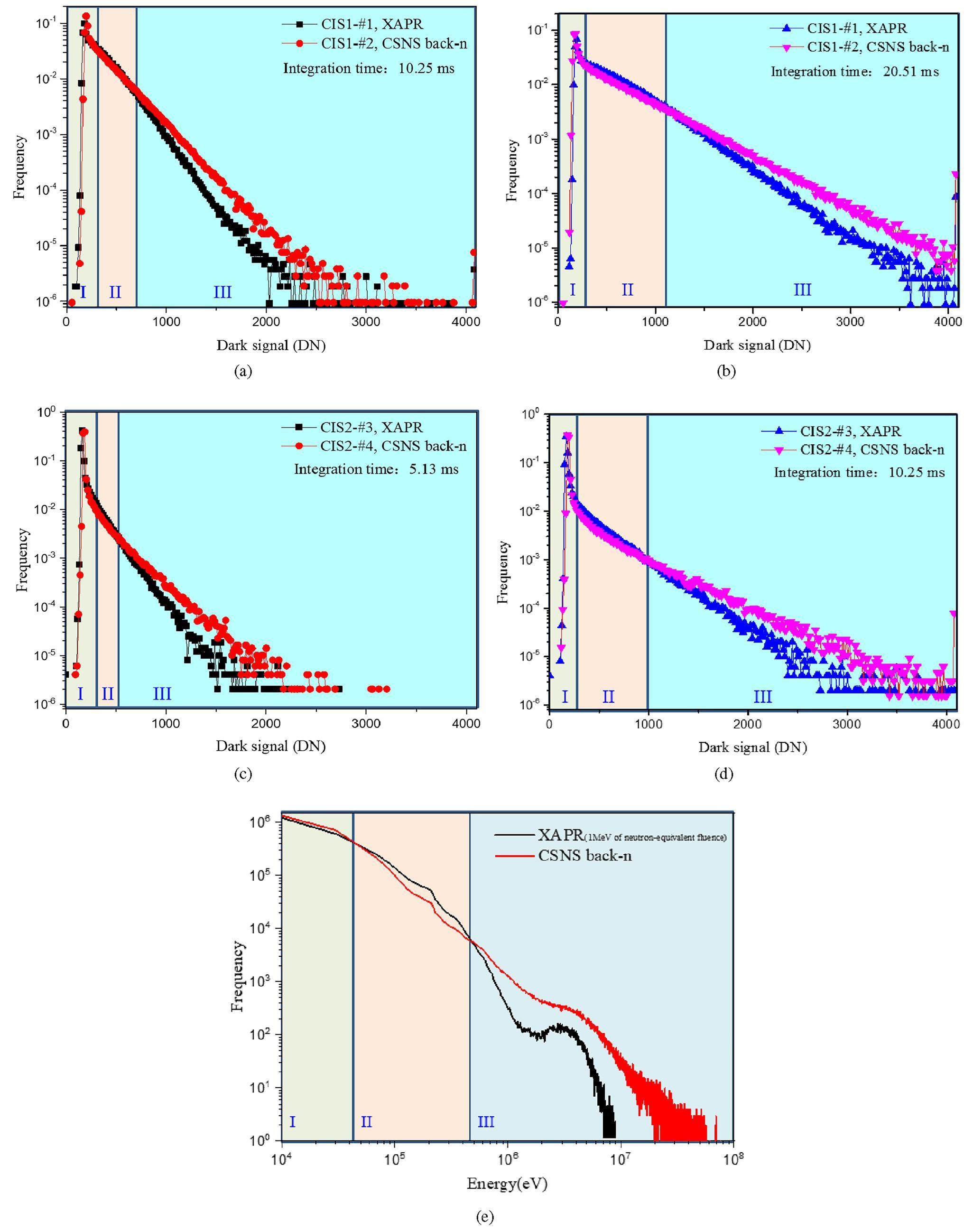
The dark signal is proportional to the dark current, which consists of surface, bulk, and diffusion currents in the CIS. After neutron irradiation, the increase in the dark current is mainly induced by the bulk current at room temperature. Bulk dark current is mainly induced by the bulk defects in SCR. The bulk defects in SCR induced by the PKA of neutrons operate as Shockley–Read–Hall recombination-generation (SRH R-G) centers and generate dark current, leading to a dark increase. The bulk current density due to bulk defects can be expressed as
Hot pixels
Hot pixels in the CIS represent pixels that generate significantly higher dark signals than normal pixels, resulting in noticeable bright spots or hot spots in the output images. The proportion of hot pixels is one of the most important parameters for evaluating the performance of CIS imaging and detection systems in radiation environments. Hot pixels may be caused by various factors such as manufacturing defects and radiation damage. After neutron irradiation, many pixels are damaged by neutrons and become hot pixels. The frequencies of hot pixels with dark signals higher than 1500 and 2000 DN after CSNS back-n and XAPR neutron irradiation are shown in Fig. 6(a) and (b), respectively. Figure 6(a) and (b), show that the CSNS back-n produces higher dark signal value pixels than the XAPR neutrons. In addition, the number of pixels with high dark signal values produced in CIS2 was greater than that produced in CIS1, which may be affected by the pixel structure of these two types of CISs. The 3D dark signal spikes of CIS1 before and after neutron irradiation are shown in Fig. 6(c). The neutron irradiation fluence is 1 × 10¹¹ n/cm2. Figure 6 shows that more high dark-signal spikes of CIS1 are observed after CSNS back-n irradiation than after XAPR neutron irradiation. This result also agrees with the results presented in Fig. 5(a)-(d).
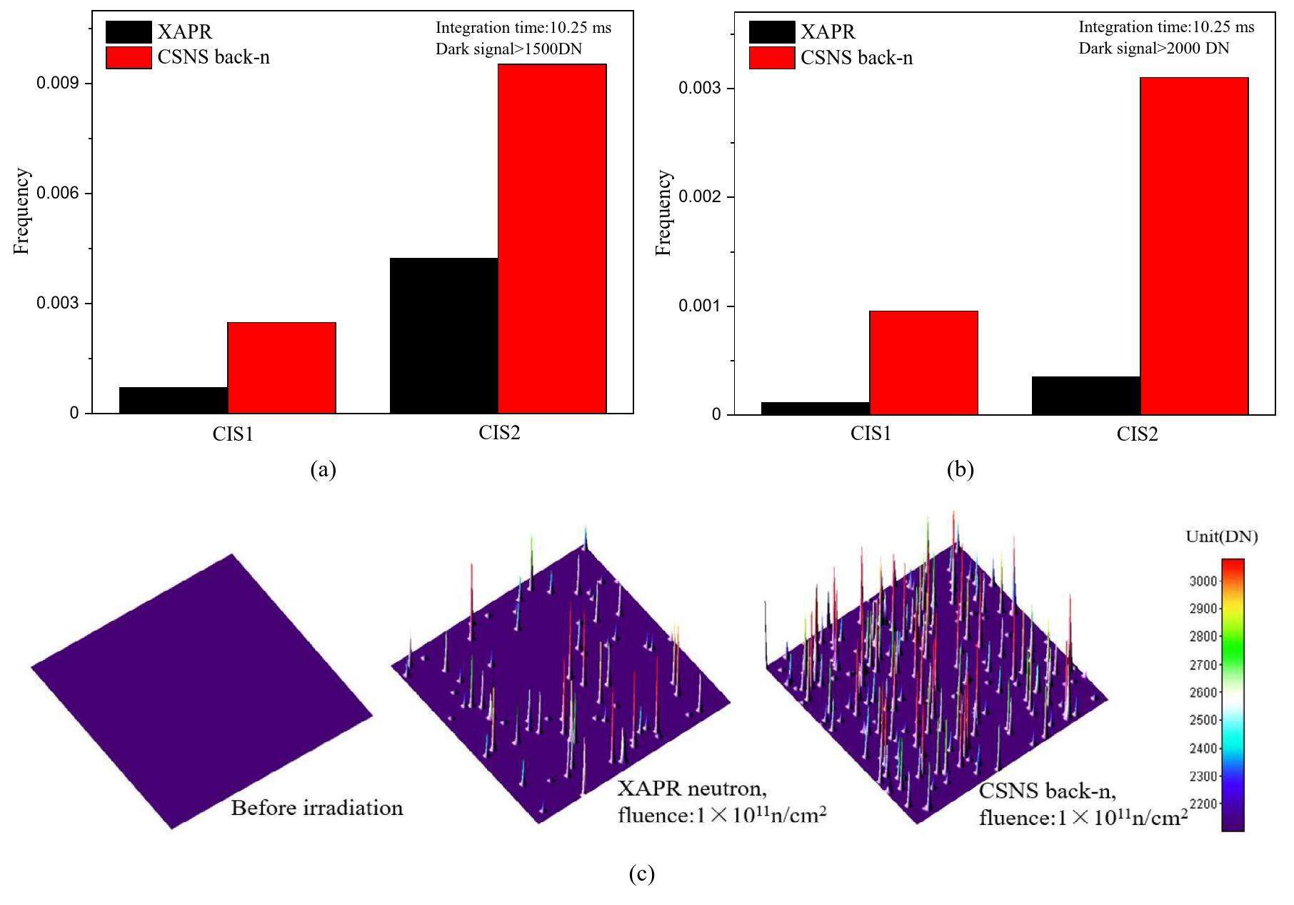
The atomic number and energy of the PKA would have a significant effect on the degree of damage to pixels. Generally, after CSNS Back-n and XAPR neutron (with an average energy of several mega electron volts) irradiation, the main types of PKAs are Si ions. For the CSNS Back-n with a wide energy range, the probability of generating a high-energy PKA is greater than that of reactor neutrons (as shown in Fig. 5(e)). A high-energy PKA produces a high density of defects and causes severe damage. Therefore, the output signal in the CSNS Back-n with a thermal pixel greater than 1500 or 2000 DN is significantly higher than that of the XAPR neutron.
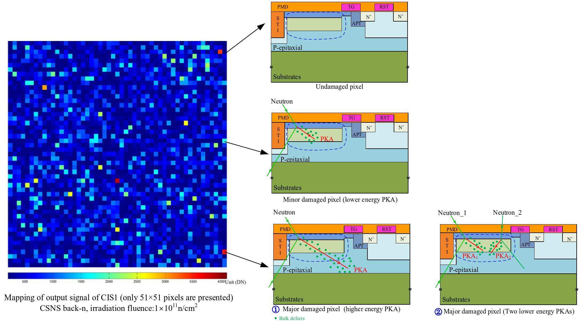
The mapping of the output signal of CIS1 after CSNS back-n irradiation and schematic of radiation damage in pixel of CIS1 are shown in Fig. 7. A dark signal of 51 × 51 pixels is presented, with a neutron irradiation fluence of approximately 1 × 10¹¹ n/cm2. Pixels of different colors represent different dark signals. Figure 7 shows that after neutron irradiation, different CIS pixels are subjected to different levels of radiation damage. In addition, some pixels remain undamaged by neutrons. The difference in dark signal from the damaged pixels of the CIS is primarily due to two aspects. First, the interaction between neutrons and the material results in different PKA energies that cause damage, and second, the same pixel is irradiated by multiple neutrons during the accumulation of a neutron irradiation fluence of 1 × 10¹¹ n/cm2. In this irradiation experiment, the CIS is unbiased, and single-displacement damage is negligible. Fortunately, similar results were observed during an in-situ radiation test of CCD [30]. Further in-situ CIS radiation tests will be conducted in our future studies.
Discussion
The CIS includes a programmable gain amplifier (PGA) array, a low-power analog-to-digital converter array, a serial periphery interface, and eight low-voltage differential signaling channels. In neutron radiation environments, TID effects are induced by accompanying gamma rays or PKAs. It is crucial to determine whether these devices are damaged by the TID after neutron radiation to analyze the degradation of the dark signal. Therefore, the conversion gain (CVG) of a CIS is measured after neutron irradiation. The CVGs of CIS1 and CIS2 remain almost unchanged before and after exposure to CSNS Back-n and XAPR neutrons [31, 32], indicating that the damage is mainly induced by the DDD effects in the pixel arrays of the CIS.
In addition, neutron irradiation in a CIS creates various defects, including point and clustered defects, in the SCR of pixels. These defects introduce energy levels within the Si bandgap and enhance thermal generation processes. There is a relationship that exists between the probabilities of generating both high-energy PKAs and neutron energy. In general, as neutron energy increases, the probability of generating high-energy PKAs also increases. This is because high-energy neutrons have high momentum and kinetic energy, which can interact with surrounding atomic nuclei, generating high-energy PKAs. As the energy of the PKAs increases, the probability of cascade collisions gradually increases, causing defects to transition from point defects to defect clusters by irradiation. This transition changes the energy levels of the defects, influencing different energy levels of device performance in various ways [33]. Generally, defects located in the middle energy level of the forbidden band have the greatest impact on the device. Therefore, the types of defects generated by neutrons of different energies may vary. In future studies, we will investigate the energy-level positions and activation energies of defects in pixel arrays produced by neutrons of varying energies.
The effects of neutron radiation on CISs have also been employed to evaluate displacement damage induced by protons in the space environment. The different results from CSNS back-n and XAPR neutrons show that similar results may be found in neutron and proton irradiation experiments with different energies. Similar results were observed in proton irradiation experiments with different energies. Therefore, further experiments should be conducted to investigate this phenomenon.
Conclusion
This study focused on examining the impact of displacement damage on the dark signal of CIS when exposed to CSNS back-n and XAPR neutrons. Both experimental and simulation methods were employed to investigate the variations in the mean dark signal, DSNU, and dark signal distribution caused by the two neutron sources. The Geant4 simulation tool was used to calculate the NIEL and PKA spectra of Si. The results revealed that the NIEL values followed the trend NIEL1 MeV > NIELCSNS > NIELXAPR.
The mean dark signal is directly correlated with the DDD. However, it is noteworthy that the DSNU of CIS following CSNS back-neutron irradiation exceeds that of CIS exposed to XAPR neutron irradiation. Higher neutron energies at the same DDD level may lead to a more pronounced DSNU and elevated hot-pixel values. Therefore, relying solely on the equivalent DDD for DSNU evaluation is insufficient. Additionally, variations in the dark signal distribution were observed, revealing three distinct regions that aligned with the predicted PKA distributions obtained through Geant4 simulations. These findings are crucial for assessing the impact of displacement damage on CIS. Future studies will involve more experiments and simulations to provide an in-depth analysis of the displacement damage effect on DSNU and the dark signal distribution of the CIS.
Gamma measurement based on cmos sensor and arm microcontroller
. Nucl. Sci. Tech. 28, 122 (2017). https://doi.org/10.1007/s41365-019-0634-yAnalyzing the transient effects of Co-60 gamma rays in a CIS by monte carlo method
. Nucl. Sci. Tech. 7, 33 (2019). https://doi.org/10.1007/s41365-017-0276xPrototype of single-event effect localization system with CMOS pixel sensor
. Nucl. Sci. Tech. 33, 136 (2022). https://doi.org/10.1007/s41365-022-01128-5X-ray detection based on complementary metal-oxide-semiconductor sensors
. Nucl. Sci. Tech. 30, 9 (2019). https://doi.org/10.1007/s41365-018-0528-4Proton, electron, and heavy ion single event effects on the HAS2 CMOS image sensor
. IEEE Trans. Nucl. Sci. 61, 4 (2014). https://doi.org/10.1109/TNS.2014.2307759High displacement damage dose effects in radiation hardened cmos image sensors
. IEEE Trans. Nucl. Sci. 17, 2781 (2020). https://doi.org/10.1109/TNS.2020.2989662Proton radiation effects on dark signal distribution of PPD CMOS image sensors: Both TID and DDD effects
. Sensors 67, 7 (2017). https://doi.org/10.3390/s17122781Displacement damage in CMOS image sensors after thermal neutron irradiation
. IEEE Trans. Nucl. Sci. 65, 11 (2018). https://doi.org/10.1109/TNS.2018.2874191Enhanced dark current generation in proton-irradiated cmos active pixel sensors
. IEEE Trans. Nucl. Sci. 49, 3 (2002). https://doi.org/10.1109/TNS.2002.1039695Review of displacement damage effects in silicon devices
. IEEE Trans. Nucl. Sci. 50, 3 (2003). https://doi.org/10.1109/TNS.2003.813197Displacement damage effects due to neutron and proton irradiations on cmos image sensors manufactured in deep submicron technology
. IEEE Trans. Nucl. Sci. 57, 6 (2010). https://doi.org/10.1109/TNS.2010.2085448Displacement damage effects in pinned photodiode cmos image sensors
. IEEE Trans. Nucl. Sci. 59, 6 (2012). https://doi.org/10.1109/TNS.2012.2224129Displacement damage equivalence of neutron and proton radiations in triple-junction gainp/gaas/ge solar cells
. IEEE Trans. Nucl. Sci. 70, 8 (2023). https://doi.org/10.1109/TNS.2023.3260117A framework for understanding displacement damage mechanisms in irradiated silicon devices
. IEEE Trans. Nucl. Sci. 53, 6 (2006). https://doi.org/10.1109/TNS.2006.885796Xi’an pulsed reactor
. Nucl. Power Eng. 23, 6 (2002). https://doi.org/10.3969/j.issn.0258-0926.2002.06.001 (in Chinese)Back-n white neutron source at csns and its applications
. Nucl. Sci. Tech. 32, 1 (2021). https://doi.org/10.1007/s41365-021-00846-6Neutron energy spectrum measurement of the back-n white neutron source at csns
. Eur. Phys. J. A. 55, 7 (2019). https://doi.org/10.1140/epja/i2019-12808-1Development of readout electronics for high resolution neutron scintillator detector
. Nucl. Sci. Tech. 46, 11 (2023). https://doi.org/10.11889/j.0253-3219.2023.hjs.46.110401Prototype motion control system for CSNS very small angle neutron scattering instruments
. Nucl. Sci. Tech. 45, 8 (2022). https://doi.org/10.11889/j.0253-3219.2022.hjs.45.080401Geant4
. http://geant4.web.cern.ch/geant4, accessedRecent developments in geant4
. Nucl. Instrum. Meth. A 835, 186–225 (2016). https://doi.org/10.1016/j.nima.2016.06.125Geant4 developments and applications
. IEEE Trans. Nucl. Sci. 53, 270–278 (2006). https://doi.org/10.1109/TNS.2006.869826Equivalent displacement damage dose for on-orbit space applications
. IEEE Trans. Nucl. Sci. 59, 6 (2012). https://doi.org/10.1109/TNS.2012.2221477New partition factor calculations for evaluating the damage of low energy ions in silicon
. IEEE Trans. Nucl. Sci. 53, 6 (2006). https://doi.org/10.1109/TNS.2006.884382Non-ionization energy loss of proton in different regions in sic
. Acta Phys. Sin. 67, 18 (2018). https://doi.org/10.7498/aps.67.20181095Displacement damage effects in irradiated semiconductor devices
. IEEE Trans. Nucl. Sci. 60, 3 (2013). https://doi.org/10.1109/TNS.2013.2261316European Machine Vision Association (EMVA), EMVA Stand 1288
, https://www.emva.org/,Modeling dark signal of cmos image sensors irradiated by reactor neutron using monte carlo method
. Sci. China-Inf. Sci. 61, 6 (2018). https://doi.org/10.1007/s11432-017-9323-0Theoretical and experimental study of the dark signal in cmos image sensors affected by neutron radiation from a nuclear reactor
. AIP Advances 7, 12 (2017). https://doi.org/10.1063/1.4999664Analysis of displacement damage effects on the charge-coupled device induced by neutrons at back-n in the china spallation neutron source
. Chin. Phys. B 32, 7 (2023). https://doi.org/10.1088/1674-1056/acac07Measurement and analysis of the conversion gain degradation of the cis detectors in harsh radiation environments
. Nucl. Instrum. Meth. A 895, 35–39 (2018). https://doi.org/10.1016/j.nima.2018.04.002Radiation effects in backside-illuminated cmos image sensors irradiated by high energy neutrons at csns-wns
. Nucl. Instrum. Meth. A 1026,Theoretical simulation of charge transfer loss degradation of cmos image sensor induced by displacement damage
. Acta Opt. Sin. 42, 7 (2022). https://doi.org/10.3788/AOS202242.0723002The authors declare that they have no competing interests.

