Introduction:
Focused hard X-ray beams have emerged as powerful tools for studying the structures and functions of complex heterogeneous systems on a microscopic scale[1]. Recent advancements in synchrotron facilities and focusing-optic manufacturing have enabled the realization of nanofocused beams[2, 3]. Using reflective, refractive, and diffractive optics, beam sizes ranging from 50 to 7 nm have been successfully achieved in hard X-ray focusing[4-6]. Based on hard X-ray nanoprobes, a variety of techniques have found important applications in multiple fields, including biology, chemistry, physics, materials science, and nanotechnology[7-12]. Presently, synchrotron facilities are operating and developing hard X-ray nanoprobe beamlines worldwide[13-19].
The hard X-ray nanoprobe beamline (BL13U) is one of the phase-II project beamlines at the Shanghai Synchrotron Radiation Facility[20-23] (SSRF). It aims to satisfy comprehensive experimental research requirements with high spatial resolution and high sensitivity detection. The scientific case for BL13U centers on spectroscopy, fluorescence, and diffraction imaging across a broad range of areas, including life, materials, and environmental sciences. The techniques available at this beamline provide spatial mapping of the elemental composition by X-ray fluorescence (XRF), speciation by X-ray absorption near-edge spectroscopy (XANES), the structural phase from nano-X-ray diffraction (nano-XRD), and phase contrast or electron density from coherent diffraction imaging (CDI) and ptychography. To meet these demands, the design of the beamline has been optimized for flexibility in energy range and focusing mode, requiring different operating modes that allow for a wide range of available X-ray energies, beam sizes, and fluxes. Two monochromators were implemented in the beamline and can be switched to provide high energy resolution or high photon flux for spectroscopy and imaging techniques, respectively. At the end station, a multilayer Kirkpatrick–Baez (KB) system, combined with a liquid nitrogen-cooled double multilayer monochromator (DMM), was adopted to achieve the designed focal spot of 10 nm at 10 keV. A total reflection KB system was installed after the liquid nitrogen-cooled double crystal monochromator (DCM) to focus the beam to 50 nm in the 5–25 keV energy range.
This paper presents the design and initial commissioning results of BL13U in terms of the beamline, experimental end-station, experimental methods, based on the multilayer KB system.
Beamline
Light source
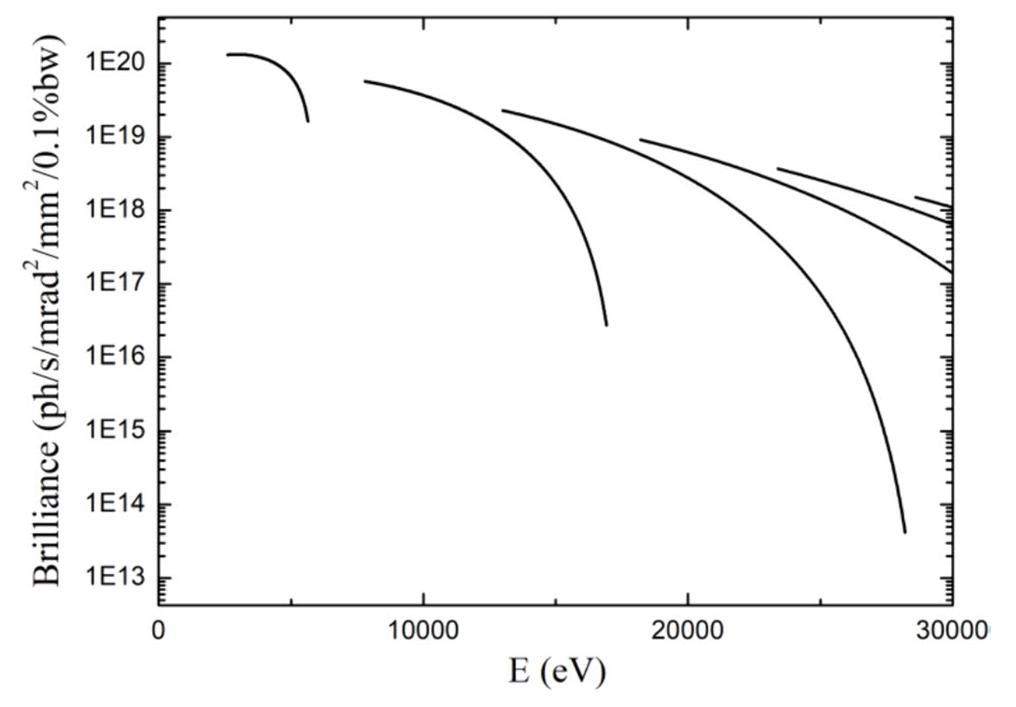
The SSRF comprises a 150 MeV electron linear accelerator, a booster that elevates the electron energy to 3.5 GeV, and a 3.5 GeV electron storage ring. To obtain continuously adjustable energy spectra, BL13U employs a U20 in-vacuum undulator as its X-ray source. This undulator has a total length of 4 m and can generate highly brilliant 1st–11th harmonics covering the entire designed energy range of 5–25 keV (minimum magnetic gap of 6 mm). The tuning curve for U20 was calculated using XOP software, as shown in Fig. 1. Calculations show that the brilliance is higher than 3.7×10¹⁹ phs/mrad2/mm2/s/ (0.1% bandwidth) at 10 keV. The specifications of the undulator are listed in Table 1.
| Parameters | Values |
|---|---|
| Storage ring energy (GeV) | 3.5 |
| Nominal design current (mA) | 300 |
| Current (operation 2023) (mA) | 200 |
| Electron beam emittance (x) (nm rad) | 4.22 |
| Electron source size (σx × σy) (μm2) | 173.1 ×10 |
| Electron source divergence (σx × σy) (μrad2) | 34.07 × 4.08 |
| Insertion device | In-vacuum undulator |
| Minimum magnetic gap (mm) | 6 |
| Number of periods | 200 |
| Period length (mm) | 20 |
| Photon energy range (keV) | 5-25 |
| Magnetic field intensity (T) | 0.84 |
| Power(K=1.57) (kW/mrad2) | 80 |
Beamline optics
The following guidelines were applied to the optical design of the hard X-ray nanoprobe beamline:
• The undulator source was focused onto the secondary source aperture by mirrors, and the beam from the second source aperture was focused onto the sample using nanofocusing KB optics.
• A DMM in conjunction with multilayer KB mirrors was used to achieve high flux at 10 nm focusing spot.
• A DCM with a total-reflection KB mirror was used to achieve higher energy resolution at 50 nm focusing spot.
A schematic overview of the beamline with the major optical components is shown in Fig. 2.
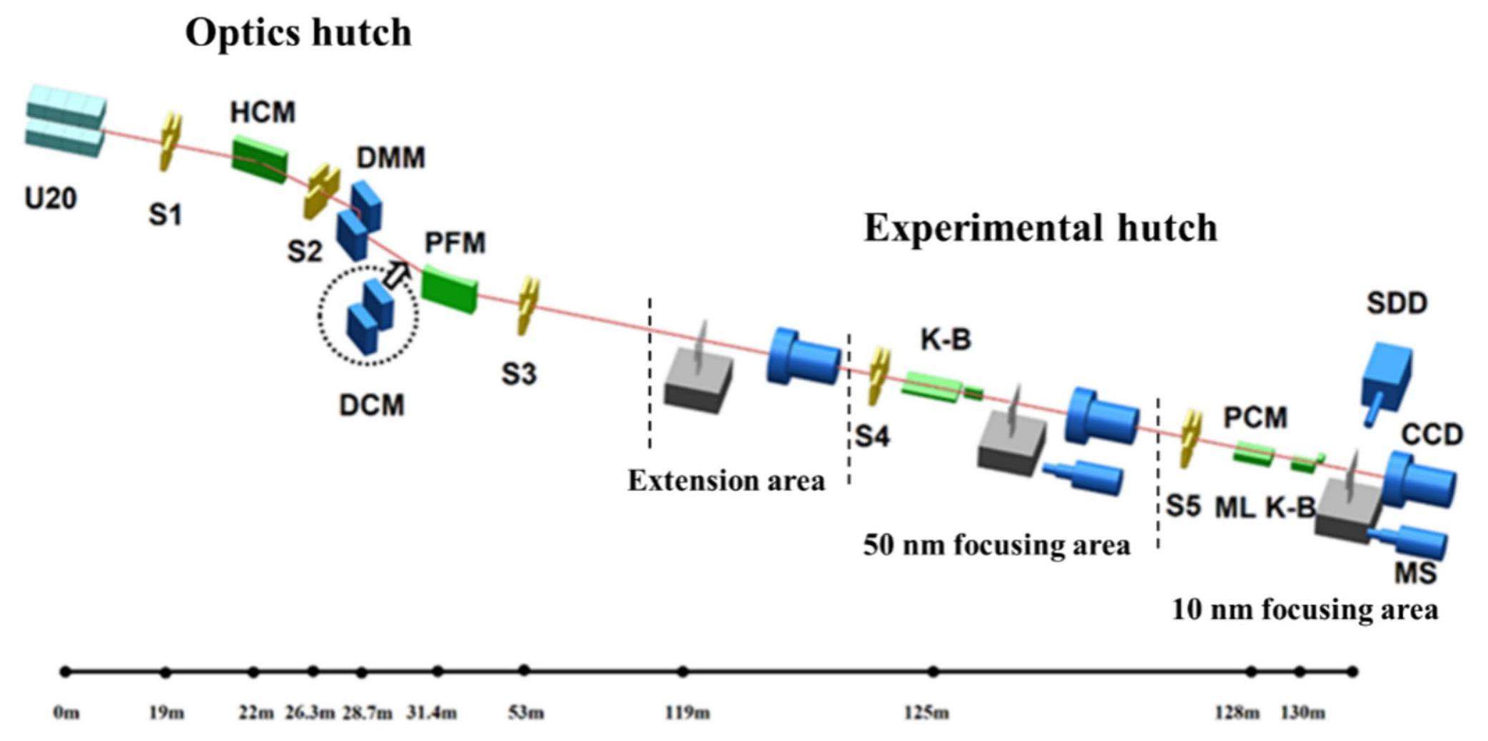
The optical layout of the beamline comprises three pairs of slits, two horizontal mirrors, and two monochromators. The photon source profile in the undulator is elliptical; thus, the main mirrors and the monochromator deflect the beam in the horizontal direction. This approach also reduces the vibrations in the vertical direction.
A water-cooled four-knife slit S1, located at 19.1 m from the source, is used to define the acceptance angle (70 µrad ×30 µrad) of the beamline and reduce the heat load on the horizontal collimating mirror (HCM, 22.5 m). The HCM (parameters listed in Table 2) is placed vertically to collimate incident X-rays in the horizontal direction. As the first optical element of the beamline, the HCM can reject high-order harmonics and reduce the thermal loading of high-energy X-rays on the monochromator crystals. To decrease the heat load on the monochromator, a four-knife slit S2 is placed at 24.7 m to limit the acceptance angle of the monochromator to 60 µrad ×20 µrad.
| Horizontal collimating mirror | Pre-focusing mirror | |
|---|---|---|
| Position (m) | 22.5 | 31.4 |
| Mirror shape | Bendable curvature circular cylinder, horizontally deflecting | Toroidal, vertically and horizontally deflecting |
| Incidence angle (mrad) | 2.5 | 2.5 |
| Mirror size (L × W) (mm2) | 800 ×10 | 650 × 5 |
| Cross-section size of beam (L × W) (mm2) | 1.3 ×0.7 | 1.3 × 0.96 |
| Slope error (μrad) | 0.5 | 0.5 |
| Micro roughness (RMS) (nm) | 0.3 | 0.3 |
| Coating | Rh/Pt, 50 nm | Rh, 50 nm |
| Substrate | Si | Si |
| Cooling system | Water-cooling system | / |
The beamline is outfitted with a pair of monochromators, each tailored for a distinct operating mode. The DMM, located 26.1 m downstream of the source, is used for the high-flux fluorescence mode. Conversely, the DCM, stationed 28.6 m from the source, is employed for the high energy resolution mode. Depending on the experimental requirements, the two monochromators (parameters listed in Table 3) can be switched.
| Double multilayer monochromator | Double-crystal monochromator | |
|---|---|---|
| Position (m) | 26.1 | 28.6 |
| Coating | Ru/C, Ni/C | / |
| Energy range (keV) | 8.3-25 (Ru/C), 5-8.3 (Ni/C) | 5-25 |
| Energy resolution (ΔE/E) | 2×10⁻² at 10 keV | 2×10⁻⁴ at 10 keV |
| Bragg angle range (°) | 0 – 2.5 | 4–24 |
| Size of crystals (L × W × H) (mm3) | 230 ×35 ×40 | 50 ×50 ×20 (first crystal) |
| 230 ×35 ×40 | 100 ×30 ×20 (second crystal) | |
| Effective size of crystals (L × W) (mm2) | 230 ×10 (two stripes) | 50 × 50 |
| 100 × 50 | ||
| Substrate | Si | Si |
| Beam offset in horizontal direction (mm) | 13.5 | 13.5 |
The multilayer monochromator can be coated with suitable multilayer pairs with different periodic thicknesses as required, which can significantly improve the flux to meet the requirements of the high-flux fluorescence mode. Two multilayers were adopted for different energy ranges: a Ru/C system with a periodic thickness of 3.1 nm for the 8.3–25 keV energy range and a Ni/C system with a periodic thickness of 3.5 nm for the 5–8.3 keV energy range, respectively. Calculations show that the reflectivities at 10 and 20 keV are higher than 75% and 85%, respectively. The multilayer stripes can be switched according to experimental requirements using a lateral motor inside the vacuum chamber. The energy resolution of the DMM is 2×10⁻² (ΔE/E) at 10 keV.
To meet the requirements of experiments such as XAFS, the energy resolution of the high-energy-resolution mode was designed to be better than 2×10⁻⁴ (ΔE/E) at 10 keV. To achieve this, a Si(111) crystal DCM is used. The energy range of the DCM is 5–25 keV, with a minimum energy step of 0.05 eV. Both the DMM and DCM are cooled by a liquid-nitrogen coolant circulation unit. The structure of the multilayer changes under thermal loads and in low-temperature environments; we conducted relevant in-situ experiments on this in the early stage[24-27]. The DMM has a much smaller grazing incidence angle (0.4°–2°) than that of the DCM (4°–24°). To ensure that both systems exhibit the same deviation of light in the horizontal direction, a constant offset of 13.5 mm is set.
After the monochromators, the toroidal prefocusing mirror (PFM, 31.4 m) focuses the beam both horizontally and vertically with respect to the secondary source aperture (S3, at 53 m). The PFM (parameters listed in Table 2) is installed vertically with a Rh surface coating and a grazing incidence angle of 2.5 mrad. The incident beam is monochromatic and the heat is very low; therefore, no special cooling is required.
The size of the secondary source aperture is defined using vertical and horizontal slit blades. The beam transverse coherence is proportional to the distance between the sample and secondary source and inversely proportional to the size of the secondary source. Thus, for XRF experiments, larger secondary source apertures are used to obtain a high photon flux, whereas for CDI experiments, coherence requires a small aperture to achieve partial or full coherence illumination.
The stability of the photon beam is the key to achieving nanofocus. The mirrors and monochromators may vibrate with changes in the thermal load over time, leading to misalignment of the photon beam on the secondary source aperture. To stabilize the beam cone before S3, a dual-frequency feedback system is implemented that reads the current signals of the beam position monitor (BPM, in front of S3) to control both the second crystals of the DMM and DCM in their pitch and roll angles and the pitch angles of the PFM using a piezoelectric actuator.
End-station setup
The experimental hutch was divided into three functional areas: the extension area, 50 nm focusing area, and 10 nm focusing area, as shown in Fig. 2. The extension area was designed for CDI and optic-testing experiments.
The 50 nm focusing area was designed to focus X-rays to 50 nm. As shown in Fig. 3(a), a total-reflection KB mirror with a fixed mirror shape was chosen as the nanofocusing optic and mounted on a high-precision manipulator inside a vacuum chamber. According to the beamline schematic, the nominal grazing incidence angle of the KB mirror is set to 2.1 mrad. The nominal focal distances from the centers of the horizontal and vertical mirrors are 45 and 160 mm, respectively, resulting in a working distance of 20 mm. This working distance provides sufficient space for in-situ environments. A laser interferometric feedback system was integrated with each mirror to maintain the distance between the mirror and sample within a change of less than 5 nm.
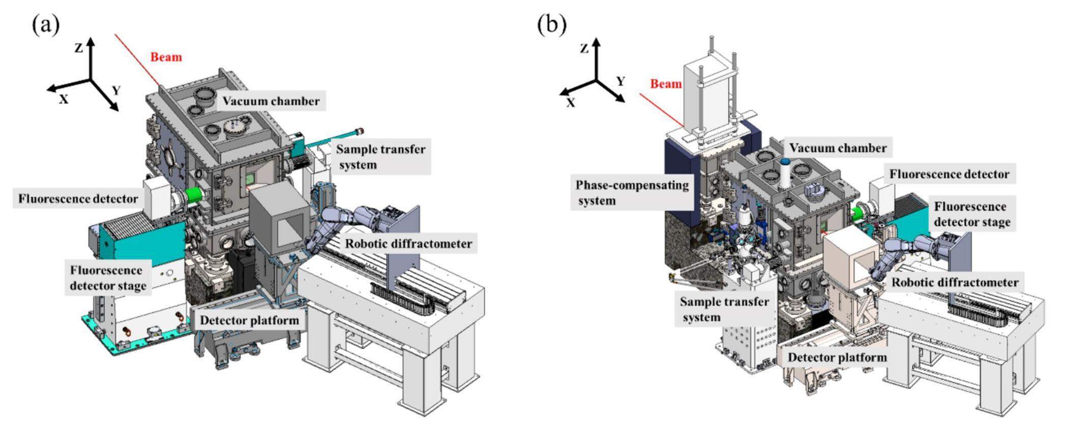
A high-precision piezoelectrically actuated sample stage (piezo stage) was mounted downstream of the total-reflection KB mirror system in the vacuum chamber. As shown in Fig. 4 (a), the sample stage is a combination of three linear translation stages and one hexapod stage, and is mounted upside down in the chamber. The base stage provides a maximum travel range of 5 cm in the X, Y, and Z directions. The upper level is a hexapod stage which can provide rotational motion with a resolution of 1 mrad, partial pendulum motion with a travel range of approximately 20°, and a travel range of 10 mm in the Z direction. The 10-mm stage provides coarse positioning in the X and Y directions. The top nanocube stage provides a 1 nm positioning resolution for nanoscanning experiments. Capacitive sensors are used to correct the movements of the piezo stage. This allows 2D mapping and tomographic measurements to be performed on a wide variety of samples. Different types of sample holders were designed to load films, capillaries, and well-designed in-situ setups. Images of the KB system and sample stage in the vacuum chamber are shown in Fig. 5.
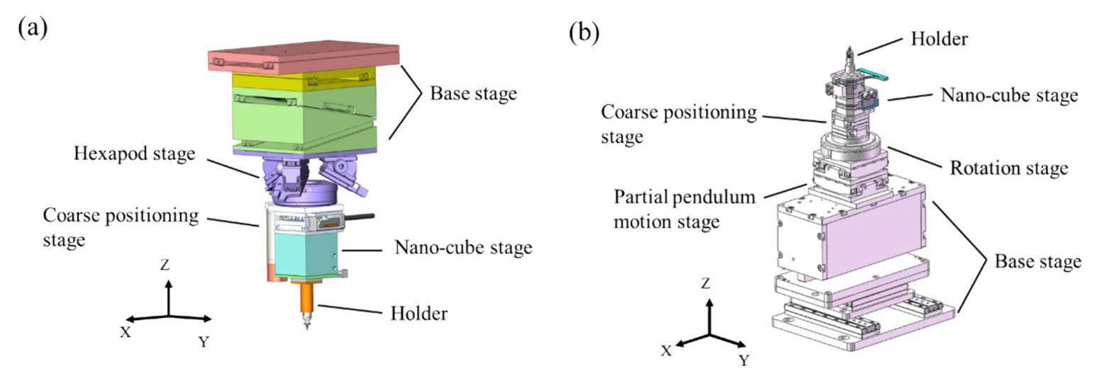
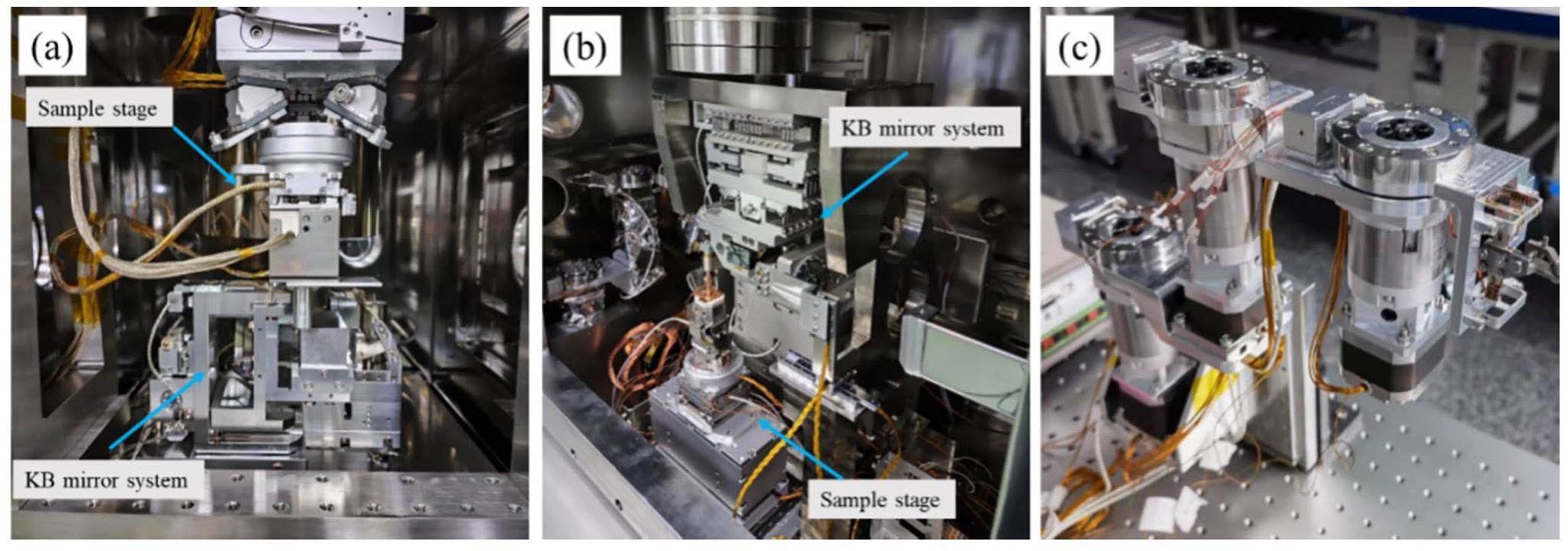
A robotic arm system (as shown in Fig. 5(c)) inside the chamber and a sample transfer system outside the chamber jointly perform automatic sample changes in the vacuum chamber. The robot can carry a load of more than 0.1 kg and achieve a positioning accuracy of 0.1 mm.
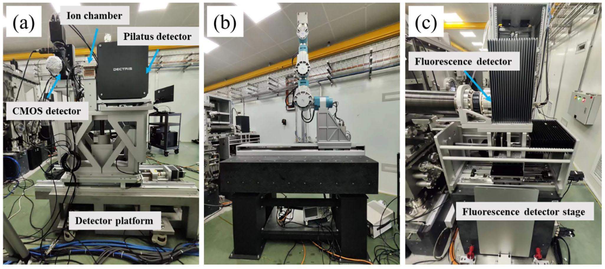
Several types of detectors are available to meet the requirements of different experiments (as shown in Fig. 6). A fluorescence detector (Vortex-ME3, Hitachi, USA) with a high-performance pulse processor (Xspress3, Quantum Detectors, UK) mounted on the fluorescence detector stage is available for nano-XRF experiments. A pixel detector (Pilatus 3 S 2M, Dectris, Switzerland), CMOS detector (ORCA-Lightning, Hamamatsu, Japan), and ion chambers (Digital Ion Chamber, OKEN, Japan) are mounted on the detector platform downstream of the vacuum chamber and can be selected for use by the motor on the platform. Bragg geometry experiments are conducted using a photon-counting pixel detector (Merlin 4X, Quantum Detectors, UK). An articulated robotic diffractometer is used to position the detector at the Bragg peak of interest. The diffractometer has seven degrees of freedom, allowing the spherical movement to reach the desired Bragg peak. In combination with the laser tracker, a positioning accuracy better than 20 μm can be achieved.
In contrast to the setup for 50-nm focusing, a phase-compensating mirror (PCM, at 129.5 m) and a multilayer KB mirror nano-focusing system (at 130 m) are utilized to achieve a 10-nm focal spot as an ultimate goal.
Compared with the total-reflection KB mirror, a fixed-surface multilayer KB mirror can increase the grazing incidence angle, resulting in a significant increase in the numerical aperture and realizing a 10-nm diffraction-limited focal spot. The downstream short mirror (horizontal focusing) determines the working distance, and the upstream long mirror (vertical focusing) has a higher fabrication difficulty and requires higher mechanical stability. Considering these aspects, the lengths of the vertical and horizontal mirror are 40 and 10 mm, respectively. The grazing incidence angle is set as 10.5 mrad.
The surface shape of the long vertical mirror is difficult to control and introduces a wavefront error that deteriorates the focal spot. To solve this problem, a phase-compensation mirror (PCM) was implemented in front of this long mirror. The PCM consists of 18 piezoelectric actuators. The voltage applied to each piezoelectric material leads to piezoelectric deformation in the transverse direction and causes the optical substrate to stretch or compress, ultimately producing the required local curvature along the meridian direction. The application of a global optimization method based on measured wavefront errors allows the precise determination of the optimal voltage distribution on the PCM[28]. This ultimately compensates for the errors originating from the KB mirror and other upstream optics. The wavefront error can be calculated from the aberrations of stripes or speckles detected by a CMOS detector mounted on a detection platform[29, 30]. To minimize the flux loss at high energies, the nominal grazing incidence angle of the Rh-coated PCM is 2.8 mrad. The parameters of the total-reflection, KB mirror, the multilayer KB mirror and the phasecompensating mirror are shown in Table 4.
| Total reflection KB mirror | Multilayer KB mirror | Phase compensating mirror | |||
|---|---|---|---|---|---|
| Position (m) | 72 | ~72 | 77 | ~77.03 | 76.55 |
| Mirror | Vertical focusing | Horizontal focusing | Vertical focusing | Horizontal focusing | Vertical focusing |
| Mirror material | Single crystal silicon | Single crystal silicon | Single crystal silicon | Single crystal silicon | Single crystal silicon |
| Substrate shape | Elliptical cylinder | Elliptical cylinder | Elliptical cylinder | Elliptical cylinder | Flat, piezoelectric deformation |
| Incidence angle (mrad) | 2.1 | 2.1 | 10.5 | 10.5 | 2.8 |
| Numerical aperture | 0.0014 | 0.0017 | 0.007 | 0.007 | |
| Substrate size (L × W × H) (mm3) | 162 ×30 ×30 | 52 × 20 ×30 | 42 × 30 ×30 | 12 × 20 ×30 | 160 × 50 ×10 |
| Active optical surface (L × W) (mm2) | 160 ×5 | 50 × 5 | 40 × 5 | 10 × 5 | 150 ×8 |
| Figure error (tangential) (nm) | PV<2 | PV<2 | PV<1 | PV<1 | PV<2 |
| Micro roughness (RMS) (nm) | <0.3 | <0.3 | <0.3 | <0.3 | <0.3 |
| Reflective coating | Rh | Rh | Ru/C | Ru/C | Rh |
| Mirror centre to focal point (mm) | 160 | 45 | 40 | 10 | / |
In the 10-nm focusing area, the high-precision piezo sample stage is a sophisticated assembly of three translation stages, one partial pendulum motion stage, and one rotation stage, as shown in Fig. 3(b). This configuration allows for a maximum travel range of 6.9 cm and a resolution of 2 nm. It’s worth noting that the detectors, detector platform, and robotic diffractometer in this area are identical to those in the 50-nm focusing area.
Experimental station
Experimental methods
Scanning nano-XRF and XRF tomography
Scanning X-ray fluorescence is a powerful technique for imaging the elemental distribution within a sample[31, 32]. Using the DMM monochromator and increasing the size of the second source aperture, we achieved a higher flux, thereby increasing the efficiency of the fluorescence experiments. The implementation of a 10–50nm focal spot can extend the spatial elemental resolution of XRF to the nanoscale, paving the way for advancements in numerous research fields. Furthermore, by performing 2D fluorescence scanning at different angles, we can achieve nanoscale imaging of 3D elemental distributions through tomographic reconstruction. However, it’s worth noting that the combination of XRF and tomography requires a substantial amount of time for data acquisition. To overcome this, a fly-scan mode has been adopted to increase the experimental efficiency[33, 34].
Diffraction method
X-ray diffraction, an important basic experimental method, is widely used to study the crystal structure of materials[35, 36]. By positioning the area detector (Pilatus detector) downstream of the sample in transmission mode, we can capture XRD patterns. Two-dimensional XRD can be realized by raster scanning the sample. Additionally, XRF and XRD can be performed simultaneously, providing a simultaneous investigation of both the crystalline structure and elemental distribution.
CDI is a lensless imaging technique capable of recovering the shape and strain of a sample[37-39]. This is achieved by analyzing the diffraction pattern of the detector using a phase-recovery algorithm[40]. Coherence is a key factor for achieving CDI. To fulfill the full coherence requirement, the second source aperture is set to 11 µm vertically and 46 µm horizontally. The balance between the signal strength and oversampling ratio of the CDI experiment is crucial and can be accomplished by adjusting the distance between the detector and the sample.
CDI can only reconstruct isolated samples, which limits its application. To overcome this, ptychography is performed. Ptychography can be regarded as the combination of CDI and scanning transmission X-ray microscopy[41]. The high-precision sample stage in BL13U fulfills the requirement for the overlapping scanning of the probe. The diffraction pattern can be captured using the detector (Merlin detector) on a robotic diffractometer. Phase retrieval algorithms[42] are used to reconstruct the electron densities of the samples.
The data acquisitions of fluorescence and ptychography have no conflict, which grants the opportunity to simultaneously obtain the elemental distribution and microstructure of the sample. Moreover, by combining this with tomography, 3D nanoscale localization of elements in a sample can provide more information for scientific research.
Absorption spectrum
The oxidation state of a given element can be investigated by analyzing the XANES. At BL13U, XANES measurements can be performed in either the transmission or fluorescence modes using an ion chamber and a fluorescence detector (Vortex-ME3), respectively. The distance between the fluorescence detector and sample can be adjusted using the fluorescence detector stage to optimize the intensity of the fluorescence signal. Furthermore, the spatial resolution of the chemical states of the elements within the sample can be determined through XANES mapping.
Control and data-acquisition system
The control system consists of software and hardware platforms. The Experimental Physics and Industrial Control System (EPICS) is used as the software platform. It provides a more efficient data communication protocol (PVAS) and more flexible data structure (pvData). Additionally, EPICS provides a rich set of C-language interface functions that can be seamlessly integrated into C- or C++-based image data processing software packages. The core of the hardware platform is a motion controller. The VME motion controller (TURBO-PMAC2-VME, DELTA TAU, US) offers a wide range of control methods, supports laser interferometer-based position encoders, and has standard PID feedback control algorithms that have been adopted as motion controllers in BL13U. The control system uses a server/client architecture. The human–computer interface platform uses computers running Linux or Windows operating systems, and the experimental and graphic processing software packages can be run on any computer on the network as required. The network system has a bandwidth of 1 GHz.
First commissioning results
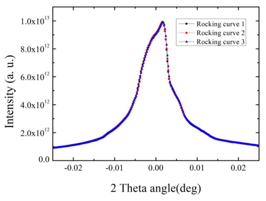
The major phase of the beamline construction was successfully completed. We have performed a focusing test for the high-flux fluorescence mode at 10 keV using the multilayer KB mirror, and the energy resolution of the DMM is approximately 0.76×10⁻² (shown in Fig. 7). Speckles have been proven to modulate wavefronts and provide sufficient wavefront information[43]. The wavefront of the focal beam was tested using X-ray speckle scanning metrology technique (SBT)[44-46]. To facilitate this, we mounted a 15000-mesh sandpaper 5-mm downstream of the focal point and positioned an Eiger detector 3591-mm downstream from the sandpaper. The test was performed by scanning the sandpaper with a step size of 200 nm over 50 steps with an exposure time of 1 s.
The rows and columns were extracted from 50 speckle images to create a series of new speckle images. The deviations between speckle images were then calculated. The local wavefront curvatures were calculated using these deviations. Quadratic integration was performed to obtain the wavefronts at the detector position. Wavefront errors in the vertical direction can be corrected using a PCM based on a global iterative algorithm[28].
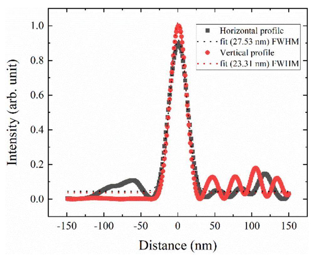
Subsequently, we employed the wavefront propagation method to calculate the focal-spot size in both horizontal and vertical directions. The final focal size was determined based on eight repeated scans. The full width at half maximum (FWHM) of the intensity profile was considered asthe focal spot size. Figure 8 illustrates the intensity profiles of the focus spot in both the horizontal and vertical directions. Based on the beamline schemes at BL13U, we achieved a focal spot of 27.53 nm in the horizontal direction and 23.31 nm in the vertical direction in the high-flux fluorescence mode at 10 keV.
Summary and conclusion
The hard X-ray nanoprobe beamline BL13U at the SSRF was designed for use in a wide range of scientific fields such as life, environmental, and materials sciences. The beamline has two different operating modes: a high-flux fluorescence mode and a high energy resolution mode, which are realized by switching the monochromator and KB mirrors. BL13U offers adjustable beam coherence owing to the modifiable size of its second source aperture. This flexibility allows it to meet the flux requirements of experiments such as XRF and XRD, as well as the coherence prerequisites of CDI and ptychography, and makes it possible for the combined use of different techniques. In addition, the high-energy-resolution mode can be used to perform XANES and in-situ experiments. We successfully constructed the beamline and tested the high-flux fluorescence mode at 10 keV with a focusing spot of approximately 30 nm. The performance results of the beamline are in good agreement with the design for a 10-nm focusing station, achieving nanoscale focusing along with a substantial flux of 5×10⁹ phs/s and a 0.76×10⁻² (ΔE/E) energy resolution. Next, we will focus on optimizing the sample experiments and adjusting the 50-nm focusing station. The equipped detectors are already capable of conducting XRF and XRD experiments. Upon completion of the high-energy-resolution mode and CDI-method testing, BL13U will be well adapted to the needs of scientific research.
Applications of synchrotron X-ray nano-probes in the field of cultural heritage
. Comptes Rendus Phys. 19, 575-588 (2018). https://doi.org/10.1016/j.crhy.2018.07.002Ptychographic characterization of a coherent nanofocused X-ray beam
. Opt. Express 28, 5069 (2020). https://doi.org/10.1364/OE.386068Combining nanofocused X-rays with electrical measurements at the NanoMAX beamline
. Crystals 9, 432 (2019). https://doi.org/10.3390/cryst908043211 nm hard X-ray focus from a large-aperture multilayer Laue lens
. Sci. Rep. 3, 3562 (2013). https://doi.org/10.1038/srep03562Erratum: breaking the 10 nm barrier in hard-X-ray focusing
. Nat. Phys. 6, 146 (2010). https://doi.org/10.1038/NPHYS1457Sub-10 nm beam confinement by X-ray waveguides: design, fabrication and characterization of optical properties
. J. Synchrotron Radiat. 19, 227-236 (2012). https://doi.org/10.1038/S0909049511051983Preliminary exploration of hard X-ray coherent diffraction imaging method at SSRF
. Acta Phys. Sin. 69, 034102 (2020). https://doi.org/10.7498/APS.69.20191586Periodic artifacts generation and suppression in X-ray ptychography
. Photonics 10, 532 (2023). https://doi.org/10.3390/photonics10050532Position-guided ptychography for vibration suppression with the aid of a laser interferometer
. Opt. Lasers Eng. 160, 107297 (2023). https://doi.org/10.1016/j.optlaseng.2022.107297Millisecond dynamics of colloidal suspension studied by X-ray photon correlation spectroscopy at the Shanghai Synchrotron Radiation Facility
. Nucl. Sci. Tech. 35, 1 (2023). https://doi.org/10.1007/s 41365-023-01358-1Three-dimensional coherent X-ray diffraction imaging of ferroelastic domains in single CsPbBr3 perovskite nanoparticles
. New J. Phys. 23, 063035 (2021). https://doi.org/10.1088/1367-2630/ac02e0In situ imaging of ferroelastic domain dynamics in CsPbBr3 perovskite nanowires by nanofocused scanning X-ray diffraction
. ACS Nano 14, 15973-15982 (2020). https://doi.org/10.1021/acsnano.0c07426The hard X-ray nanoprobe beamline at diamond light source
. J. Synchrotron Radiat. 28, 1006-1013 (2021). https://doi.org/10.1107/S1600577521002502NanoMAX: the hard X-ray nanoprobe beamline at the MAX IV Laboratory
. J. Synchrotron Radiat. 28, 1935-1947 (2021). https://doi.org/10.1107/S 1600577521008213Capabilities of time-resolved X-ray excited optical luminescence of the Taiwan Photon Source 23A X-ray nanoprobe beamline
. J. Synchrotron Radiat. 27, 217-221 (2020). https://doi.org/10.1107/S16000577519013675Hard X-ray nanoprobe: a scanning hard X-ray microscopy beamline offering multi-modal imaging capabilities at 10 nm. SPIE Optical Engineering + Applications
.ID16B: a hard X-ray nanoprobe beamline at the ESRF for nano-analysis
. J. Synchrotron Radiat. 23, 344-352 (2016). https://doi.org/10.1107/S1600577515019839Hard X-ray nanoprobe at beamline P06 at PETRA III
. Nucl. Instrum. Meth. Phys. Res. Sect. A Accel. Spectrometers Detect. Assoc. Equip. 616, 93-97 (2010). https://doi.org/10.1016/j.nima.2009.10.094Optical design and multi-length-scale scanning spectro-microscopy possibilities at the Nanoscopium beamline of Synchrotron Soleil
. J. Synchrotron Radiat. 22, 1118-1129 (2015). https://doi.org/10.1107/S1600577515009364Current status and progresses of SSRF project
. Nucl. Sci. Tech. 19, 1-6 (2008). https://doi.org/10.1016/S 1001-8042(08)60013-5Progress and future of Shanghai synchrotron radiation facility
. J. Vac. Soc. Jpn. 59, 198-204 (2016). https://doi.org/10.3131/JVSJ2.59.198Shanghai synchrotron radiation facility
. Natl. Sci. Rev. 1, 171-172 (2014). https://doi.org/10.1093/nsr/nwt039The protein complex crystallography beamline (BL19U1) at the Shanghai Synchrotron Radiation Facility
. Nucl. Sci. Tech. 30, 170 (2019). https://doi.org/10.1007/s 41365-019-0683-2Structural characterization and low-temperature properties of Ru/C multilayer monochromators with different periodic thicknesses
. J. Synchrotron Radiat. 22, 1379-1385 (2015). https://doi.org/10.1107/S1600577515017828Thermal and temporal stability of nitridated Ru/B4C multilayer for high flux monochromator application
. inIn situ GISAXS study on the temperature-dependent performance of multilayer monochromators from the liquid nitrogen cooling temperature to 600℃
. Appl. Surf. Sci. 508, 144838 (2020). https://doi.org/10.1016/j.apsusc.2019,144838Temperature-dependent thermal properties of Ru/C multilayers
. J. Synchrotron Radiat. 24, 975-980 (2017). https://doi.org/10.1039/d0nr02260hA piezoelectric deformable X-ray mirror for phase compensation based on global optimization
. J. Synchrotron Radiat. 26, 729-736 (2019). https://doi.org/10.1107/S1600577519003047Influence of diffuser grain size on the speckle tracking technique
. J. Synchrotron Radiat. 27, 146-157 (2020). https://doi.org/10.1107/s1600577519015200Influence of photon beam and motor vibrations on at-wavelength X-ray speckle scanning metrology
. Front. Phys. 10, 864985 (2022). https://doi.org/10.3389/fphy.2022.864985Visualization of a lost painting by vincent van gogh using synchrotron radiation based X-ray fluorescence elemental mapping
. Anal. Chem. 80, 6436-6442 (2008). https://doi.org/10.1021/ac800965gVisualizing mineralization processes and fossil anatomy using synchronous synchrotron X-ray fluorescence and X-ray diffraction mapping
. J. Roy. Soc. Interface. 17, 20200216 (2020). https://doi.org/10.1098/rsif.2020.0216High-speed three-dimensional imaging at the nanoscale via fly-scan ptycho-tomography
. Microsc. Microanal. 26, 1006-1008 (2020). https://doi.org/10.1017/S1431927620016645On-the-fly scans for X-ray ptychography
. Appl. Phys. Lett. 105, 251101 (2014). https://doi.org/10.1063/1.4904943Probing the deformation and fracture properties of Cu/W nano-multilayers by in situ SEM and synchrotron XRD strain microscopy
. Surf. Coat. Technol. 320, 158-167 (2017). https://doi.org/10.1039/d0nr02260hProgress of in situ synchrotron X-ray diffraction studies on the mechanical behavior of materials at small scales
. Prog. Mater. Sci. 94, 384-434 (2018). https://doi.org/10.1016/J.SURFCOAT.2017.01.065Coherent X-ray diffraction imaging
. IEEE J. Sel. Top. Quantum Electron. 18, 399-410 (2012). https://doi.org/10.1109/jstqe.2011.2157306Coherent X-ray diffraction imaging of strain at the nanoscale
. Nat. Mater. 8, 291-298 (2009). https://doi.org/10.1038/nmat2400Coherent diffraction imaging of nanoscale strain evolution in a single crystal under high pressure
. Nat. Commun. 4, 1680 (2013). https://doi.org/10.1038/ncomms2661Reconstruction of a complex-valued object from the modulus of its Fourier transform using a support constraint
. J. Opt. Soc. Am. A 4, 118-123 (1987). https://doi.org/10.1364/JOSAA.4.00018X-ray ptychography
. Nat. Photonics 12, 9-17 (2018). https://doi.org/10.1038/S41566-017-0072-5PyNX.Ptycho: a computing library for X-ray coherent diffraction imaging of nanostructures
. J. Appl. Crystallogr. 49, 1842-1848 (2016). https://doi.org/10.1107/S1600576716012279Deep learning for estimation of Kirkpatrick–Baez mirror alignment errors
. Nucl. Sci. Tech. 34, 122 (2023). https://doi.org/10.1007/s41365-01282-4Advanced in situ metrology for X-ray beam shaping with super precision
. Opt. Express 23, 1605-1614 (2015). https://doi.org/10.1364/OE.23.001605Auto-alignment of X-ray focusing mirrors with speckle-based at-wavelength metrology
. Opt. Express 26, 26961 (2018). https://doi.org/10.1364/OE.26.026961Extraction of medium-spatial-frequency interfacial waviness and inner structure from X-ray multilayers using the speckle scanning technique
. Opt. Mater. Express 9, 2878 (2019). https://doi.org/10.1364/OME.9.002878The authors declare that they have no competing interests

