Introduction
Superconducting radio-frequency (SRF) cavities are widely used in modern particle accelerators owing to their high accelerating field, large beam aperture, and remarkably low RF loss [1]. The performance of SRF cavities is commonly characterized by the unloaded quality factor Q0, which is inversely proportional to the average surface resistance Rs, maximum available accelerating field Eacc, and operational stability against thermal breakdown, helium pressure fluctuation, mechanical vibration, and Lorentz force detuning. Owing to its high superconducting transition critical temperature and highest lower critical magnetic field among elementary superconductors, niobium (Nb) is the material of choice for manufacturing SRF cavities. Over the past several years, efforts within the SRF community have primarily focused on attaining high Q0 and Eacc for the SRF cavities by developing advanced surface processing techniques (e.g., nitrogen doping [2-6], nitrogen infusion [5, 7, 8], mid-temperature baking [9-13] and plasma cleaning [14, 15]), researching the alternative materials (e.g., Nb3Sn, NbN and MgB2), and exploring the RF loss mechanisms. Currently, bulk Nb cavities exhibit the best overall Q0 and Eacc among the materials suitable for SRF applications. However, the limited thermal conductivity of Nb at cryogenic temperature (i.e., ~ 60 W/(m·K) and ~ 10 W/(m·K) at 4.2 K and 2 K, respectively) necessitates the wall thickness of the bulk Nb cavities ranging from 3 mm to 5 mm, leading to the cavities with low mechanical stability, particularly for the low-beta cavities. Furthermore, both Q0 and Eacc in the high accelerating field regime are primarily constrained by thermal breakdown and are below the theoretical limits determined by the superheating magnetic field Hsh of Nb.
With the commissioning of the accelerators that utilize low-beta bulk Nb cavities, such as the Soreq Applied Research Accelerator Facility (SARAF) at the Soreq Nuclear Research Center in Israel [16] and the Chinese ADS Front-end Demo Linac (CAFe) at the Institute of Modern Physics, Chinese Academy of Sciences (IMP, CAS) [17-21], the significance of the operational stabilities, specifically mechanical and thermal stability, of the SRF cavities has become more pronounced. Approximately 43% of the operational instability of CAFe between 2018 and 2019 was attributed to the low-beta bulk Nb cavity system [18]. Typical phenomena are as follows. One cavity in the cryomodule experiences thermal breakdown induced by the field-emission effect, resulting in helium (He) fluctuation in the cryogenic system. This is followed by frequency detuning of the other cavities in the same cryomodule, and subsequently triggering the RF switch-off of the cavities that underwent frequency detuning, thereby disabling the operation of the accelerator. Traditional methods for improving the mechanical stability of bulk Nb cavities involve the design and fabrication of stiffened structures on their outer surfaces. However, this introduces complexity into the manufacturing and assembly of the cavities. Moreover, the performance of cavities with stiffened structures is still affected by the low thermal conductivity of Nb at cryogenic temperatures.
The copper-niobium (Cu-Nb) superconducting cavities technique is considered to be the most promising approach to enhance both the mechanical and thermal stability of the bulk Nb cavities for several reasons. (1) The interaction between the RF field and the cavity material occurs only within the upmost layer of the cavity's inner surface (~ tens of nanometers), thereby enabling the use of a considerably thinner Nb layer to sustain the RF field inside the cavities. Consequently, the material cost of Nb is reduced. (2) The use of oxygen-free high-purity copper (Cu), which possesses a significantly higher thermal conductivity of ~ 400 W/(m·K) compared to that of Nb of ~ 60 W/(m·K) at 4.2 K, facilitates the efficient transfer of thermal deposition related to the RF loss and the vacuum electron loaded effect inside the cavity to the cooling medium. This mitigates the thermal breakdown at high accelerating gradient and further improves the Q0 and Eacc of the cavity. (3) Employing a thin Nb layer backed by a thick Cu layer as the cavity wall enhances the mechanical stability of the cavity. Two types of Cu-Nb superconducting cavities: Nb thin films on Cu cavities and bimetallic Cu-Nb cavities (Cu-Nb composite cavities), have been explored within the SRF community to improve the mechanical stability, thermal stability against thermal quenching, and cost-effective mass production of SRF cavities. The formation of Nb thin films on Cu cavities via sputtering technology was invented at CERN in 1980 [22], and consequently successfully applied for the mass production of cavities for projects such as LEP, LHC, and HIE-ISOLDE at CERN [23, 24], and the ALPI linac at INFN-LNL [25]. Nb thin films on Cu cavities were found to exhibit higher Q0 values because of the lower Bardeen-Cooper-Schrieffer (BCS) surface resistance and lower surface resistance sensitivity to the residual magnetic field [23]. In terms of the overall RF performance, a gap still exists between the Nb thin films on the Cu and bulk Nb cavities. Ongoing R&D efforts are focused on further enhancing the radio frequency (RF) performance of Nb thin films on Cu cavities, including the improvement of Nb thin film quality using advanced coating techniques, Cu substrate quality using seamless technology, internal welding and electropolishing, and optimization of the cooling conditions of Nb thin films on Cu cavities [26-28].
The Cu-Nb composite cavities can exploit the high accelerating gradient recipes developed for the bulk Nb cavity, theoretically ensuring that its RF performance is comparable to that of the bulk Nb cavities. However, to date, only a few laboratories have explored Cu-Nb composite cavities. For instance, 46 Cu-Nb composite quarter-wave resonators (QWR) have been developed and operated as heavy-ion energy boosters at the Japan Atomic Energy Research Institute since 1994. The inner conductor and top shorting plate of the QWRs cooled by liquid He were made of high-purity Nb, and the outer conductor with an oval cylindrical shape was made of a Cu-Nb composite material and cooled via thermal conduction of the Cu layer. Cu (8 mm)-Nb (2 mm) composite sheets were manufactured using the explosive bonding technique. The average Eacc was 6.5 MV/m with an RF input power of 4 W. The QWRs demonstrated robust operating stability against He pressure fluctuations after a stiffening support was added to the top endplate. However, the fabrication experience revealed that the welding of the confronting Nb ends of the Cu-Nb composite sheets was not reliable [29]. In 1994, the High Energy Accelerator Research Organization (KEK) proposed a Cu-Nb composite seamless TESLA-shaped cavity for cost-effective mass production and then developed the cavities in collaboration with the National Institute for Nuclear Physics (INFN) in Italy, Deutsches Elektronen Synchrotron (DESY), and Jefferson Lab, based on spinning (INFN) and hydro-forming (DESY) techniques [30]. The Cu-Nb composite seamless TESLA-shaped single-cell cavity manufactured using a hydroforming technique with explosively bonded Cu–Nb composite tubes out of a 1 mm thick seamless Nb inner tube and 3 mm thick outer Cu tube achieved an excellent high-gradient performance of ~ 40 MV/m even without undergoing an electropolishing process. The Q0 drop induced by the frozen flux generated by the Seebeck effect following the quench event was observed. It appears that an optimization of the Nb thickness was crucial for mitigating the Q0 drop of the Cu-Nb composite cavities. Researchers from IPN Orsay in France presented a stiffening method for SRF cavities that involved thermally spraying Cu onto the outer surfaces of bulk Nb cavities [31]. Their results revealed a 35% improvement in the Lorentz detuning factor K of the cavity with the addition of Cu stiffening. The porosity rate of the Cu layer and Cu oxidation during the Cu-layer deposition process affected the mechanical and thermal properties of the Nb-Cu structure. Gianluigi Ciovati et al. from the Jefferson Lab reported their research on a multimetallic conduction-cooled SRF cavity, wherein the cavity had a ~ 2 μm-thick layer of Nb3Sn on the inner surface of a bulk Nb cavity and a bulk Cu layer of 5 mm in thickness deposited on the outer surface via electroplating. Their results demonstrated that the multimetallic conduction-cooled cavity, which achieved an accelerating gradient of 6.5 MV/m, exhibited high thermal stability, which was attributed to the thick Cu layer with high thermal conductivity [32]. Further research is essential to explore the engineering applications of the Cu-Nb composite cavities with a high accelerating gradient and Q0 using reliable technical methods, particularly for low-beta SRF cavities.
The China Initiative Accelerator Driven System (CiADS) project for nuclear waste transmutation sets stringent reliability requirements for the superconducting linac. These requirements include a beam-trip duration tolerance of less than 10 s, a beam trip ranging from 10 s to 5 min that does not exceeding 2500 counts per year, and beam trips lasting more than 5 min that must be less than 50 counts per year [18]. Consequently, the fabrication of SRF cavities with exceptionally high mechanical and thermal stabilities is essential and challenging. As mentioned above, theoretically, the Cu-Nb composite superconducting cavities have excellent potential for high thermal and mechanical stability to satisfy the high-reliability requirements of the superconducting linac. The spinning and hydro-forming technologies are difficult to be applied for the fabrication of the low-beta SRF cavities, such as quarter-wave resonators, half-wave resonators, spoke cavities, etc. Therefore, researchers at the IMP have been exploring Cu-Nb composite cavities through various methods since 2018 [33, 34]. These include the development of single-cell elliptical cavities based on Cu-Nb composite sheets manufactured using explosive bonding technology and hot isostatic technology, as well as back-coating Cu onto the outer surface of a low-beta bulk Nb cavity using electroplating technology. This study reports the details of our exploration, including the fabrication process, cryogenic RF performance characterization, and mechanical stability verification of the Cu–Nb composite cavities.
Cu-Nb composite cavities made of the Cu-Nb composite sheets
By utilizing the traditional manufacturing method for bulk Nb cavities, several 1.3 GHz single-cell elliptical cavities based on Cu-Nb composite sheets were fabricated and studied to evaluate the reliability of the manufacturing method and the performance of the Cu-Nb composite cavity. The detailed manufacturing processes are as follows: preparation of Cu-Nb composite sheets, deep drawing of the parts made of Cu-Nb composite sheets (i.e., half-cell cups), trimming, Cu removal in the electron beam welding area of the parts using machining and nitric acid solution, and electron beam welding of the parts together. In our study, cavities based on Cu-Nb composite sheets fabricated via explosive bonding technology and hot isostatic technology were explored, and Nb beam tubes were used.
Cavities based on the explosively bonding technology
Two 1.3 GHz single-cell elliptical cavities based on explosively bonded Cu-Nb composite sheets were fabricated, as shown in Fig. 1. Additional stiffening was welded to the outer surfaces of the cavities for reliable transportation, and the weld region at the equator was not patched with Cu. The procedure for manufacturing explosively bonded Cu-Nb composite sheets is as follows: (1) Nb sheets with a residual resistivity ratio (RRR) > 300 and Cu sheets with purity > 99.99% were fabricated, followed by surface processing through grinding, sand-blasting, and cleaning; (2) one surface of the Nb sheet was protected by a PVC film, while the opposite surface was stacked onto the Cu sheet; (3) the explosive material was evenly distributed on the PVC protection film surface, which was then detonated, forming the Cu-Nb composite sheet; and 4) the Cu-Nb composite sheet was finished. The thicknesses of the Cu and Nb layers used for cavity manufacturing were ~ 6.8 mm and ~ 1.5 mm, respectively. Note that the Cu-Nb boundary of the composite sheets has a wavy structure with a peak-to-peak amplitude of ~ 0.5 mm. The average Nb thickness in the welding areas at the irises and equator of the Cu-Nb composite half-cell cups were 1.08 mm and 1.48 mm, respectively. No obvious defects were observed on the inner surfaces of the cavities during camera inspection. However, after removing ~ 28 μm of the Nb material via buffer chemical polishing (BCP) with an acid mixture with a density of ~ 1.5 kg/L containing HF (40% wt.), HNO3 (65-68% wt.), and H3PO4 (85% wt.) at a volume ratio of 1:1:2 at temperatures below 12 ℃, unreliable welding was observed. Certain sections of the Nb wall at the edge of the welding seam were etched through both the irises and equator. Figure 1 (right) presents an example of a BCP etched at this position. These leaks may be attributed to the contamination of Nb at the leaky position by Cu, or the uneven filling of Nb in the wavy structure at the welding edge induced by welding stress. A considerably smaller peak-to-peak amplitude of the wavy structure by optimizing the explosive bonding conditions or using another technology is required to render the welding of Cu-Nb composite cavities easier and more reliable.
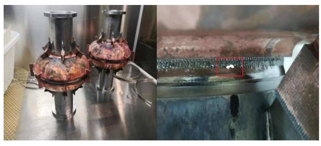
Cavities based on the hot isostatic pressure (HIP) technology
Motivated by the pursuit of a considerably smaller wavy structure at the Cu-Nb interface of the composite sheet for reliable welding, the Cu-Nb composite sheets were manufactured by HIP technology in collaboration with Advanced Technology & Materials Co., Ltd. in Beijing. Nb sheets with a residual resistivity ratio (RRR) > 300 and Cu sheets with purity > 99.99% were used for the HIP process. The procedure involved stacking the Nb sheet on the Cu sheet and sealing them in a vacuum using a steel jacket. This was then pressed for 3 hours in argon gas at a temperature of 800 ℃ and pressure of 100 MPa. Finally, the steel jacket was removed. Sample studies demonstrated that the wavy structure was eliminated, the RRR of Nb after the HIP process was ~ 286, and a tensile strength between Cu and Nb of ~ 180 MPa was achieved. Subsequently, two 1.3 GHz single-cell elliptical cavities, labeled Nb-Cu composite cavities 1 and 2, were fabricated, followed by surface processing and cryogenic tests to evaluate their RF performance and mechanical properties.
The surface processing comprised ~ 117 μm and ~ 162 μm Nb material removal for cavities 1 and 2 using a BCP with an acid mixture of density ~ 1.5 kg/L containing HF (40% wt.), HNO3 (65-68% wt.) and H3PO4 (85% wt.) at a volume ratio of 1:1:2 at the temperature below 12 ℃, respectively; Vacuum furnace outgassing at 600 ℃ for 10 hours, additional ~ 29.9 μm and ~ 20.4 μm Nb material removal for the cavity 1 and the cavity 2 by BCP, respectively; Baking at 120 ℃ for 48 h in clean room, another ~ 11.3 μm and ~ 12.1 μm material removal for the cavity 1 and the cavity 2 by BCP, respectively; high-pressure ultra-pure water rinsing, followed by another baking at 120 ℃ for 48 hours in clean room. Note that, the thickness of the Cu layer and the Nb layer was ~ 6.8 mm and ~ 1.5 mm before the surface processing, respectively.
Previous studies have revealed that the cooling dynamics at the Tc crossing of Nb affect the RF performance of bulk Nb cavities, that is, the temperature gradient along the cavity wall influences the magnetic flux expulsion efficiency [35-37]. The cooling dynamics of the bulk Nb cavity assembly affect the magnetic field generation in the cavity volume owing to the Seebeck effect [38, 39]. Limited results on the influence of the cooling dynamics at the Tc crossing of Nb on the performance of the Cu-Nb composite cavity have been reported. The research by Pashupati Dhakal et al. on the effect of cooldown on the performance of a Nb-Cu clad superconducting cavity reported that the temperature gradients during Tc crossing up to ~ 50 K/m exerted a negligible impact on the residual resistance of the cavity [40]. It is believed that additional attention to the cooling dynamics at the Tc crossing of Nb is necessary for the Cu-Nb composite cavities because the existence of the Cu–Nb bimetallic structure complicates the cooling of the Nb wall at the Tc crossing of Nb both during the cooldown process from room temperature and recovered from the localized quench. A temperature difference on the Cu–Nb cavity wall induces a thermoelectric voltage, and the magnetic flux density generated by the thermal current may be trapped in the Nb during Tc crossing. Further, the trapped flux interacting with the RF field inside the cavity results in additional RF loss, degrading the Q0 of the cavity. Therefore, the Seebeck effect on the performance of the Cu-Nb cavity was studied in detail in our cryogenic experiment.
Experimental setup
In the cryogenic testing experiments, each cavity was equipped with four temperature sensors and one magnetic flux density sensor. The setup of the cryogenic test is shown in Fig. 2. Considering the instrument setup of the Nb-Cu composite cavity 2 as an example (Fig. 2 (right)), four Cernox sensors (Model: CX-1030-CU-HT-1.4L) labeled T5-T8 were used to monitor the temperature on the outer surface of the cavity 2: T5 and T8 were located at the lower and upper beam tube, respectively, while the T6 and T7 were attached to the equator. A Bartington single-axis fluxgate sensor parallel to the beam axis and oriented downward was positioned at the equator to detect the magnetic flux density around the cavity during cooldown, RF testing, and warmup processes. It was accompanied by two temperature sensors. The stiffening at the equator and iris regions was not removed during our tests; however, most of the stiffening was loosened from the surface of the cavities after 600 ℃ for 10 hours of furnace outgassing. This is because of the different coefficients of thermal expansion of Nb and Cu. During the tests, the groove in the equator region was not patched with Cu. The tests were conducted in the vertical test dewar at the IMP, where the background magnetic flux density amplitude in the cavities' volume under test was less than 15 mGs.
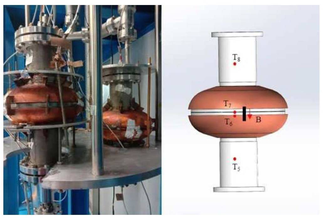
Four cooldowns with varying cooling rates and subsequent RF tests at 2 K were conducted as the following experimental procedures. (1) The cavities were cooled down to 17 K from 300 K and held for 30 min. (2) The cavities were cooled down to 2 K using the standard cooling procedure at IMP, and the Q0 versus Epk curve was measured at 2 K. (3) The cavities were warmed up to a specific temperature ranging within 10–20 K and kept for 30 min. (4) The cavities were cooled down with a certain cooling condition to 2 K, and the Q0 versus Epk curve was measured at 2 K. (5) Steps (3) and (4) were repeated twice under different cooldown conditions. In addition, the Q0 degradation of the cavity after recovery from quench events was also studied.
Result and discussion
Figure 3 presents the RF test results for the two cavities in different cooldown experiments. Epk, which is limited by the thermal breakdown of ~ 42 MV/m and ~ 50 MV/m, was obtained for cavities 1 and 2, respectively. Both cavities exhibited a Q0-slope and Q0 was less than 1×10¹⁰. As shown later, we observed that the magnetic flux density was generated and trapped during the Tc crossing of Nb in cooldown process. This is owing to the Seebeck effect of the Cu-Nb bimetallic structure, which degraded the RF performance of the cavities.
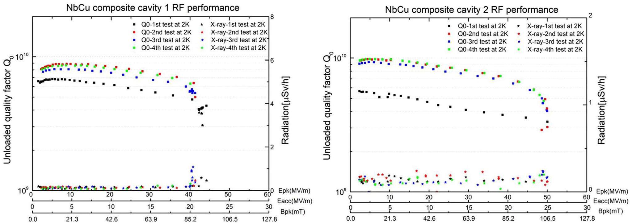
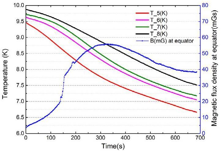
In the subsequent sections, the data from cavity 2 are mainly reported to illustrate the influence of the cooling dynamics and quench events on the RF performance of the Cu-Nb composite cavity, as cavity 2 did not exhibit any field emission effect. Figure 4 shows an example of the measured temperature and magnetic flux density as functions of time in the 1st cooldown experiment. Table 1 lists the cooling parameters of cavity 2 in different cooling experiments, indicating a positive correlation between the cooling rate and the temperature difference between the lower and upper beam tubes. The magnetic flux density at the equator during the cooling process in the temperature ranged within T5 of 9.5 K and T8 of 9.0 K, as shown in Fig. 5. This indicates that the magnetic flux density induced by the thermal current was affected by the cooling dynamics. A higher cooling rate resulted in a larger magnetic flux density, which was attributed to the more inhomogeneous cooling of the Cu-Nb composite cavity wall under a large cooling rate. Note that, the data shown in Fig. 5 includes the background magnetic flux density of ~ -14.95 mGs. In the fast cooling experiment with a cooling rate of approximately 0.258 K/min, a magnetic flux density of ~ 40 mGs was observed at the cavity equator during Tc crossing of Nb. Further, certain magnetic flux densities were trapped in Nb in the superconducting state, resulting in the lower Q0 versus Epk curve shown in Fig. 3 (right) via filled black squares. Figure 6 shows the dependence of Q0 and the surface resistance Rs of cavity 2 at Epk of ~ 10 MV/m and 2 K on the cooling rate. The surface resistance Rs exhibited certain saturation at a lower cooling rate owing to the lower magnetic flux density induced by the thermal current, and was trapped in the Nb material with a lower cooling rate. Therefore, to obtain a high Q0 for the Cu-Nb composite cavity, a lower cooling rate at the Tc crossing of Nb is preferred.
| 1st cooldown | 2nd cooldown | 3rd cooldown | 4th cooldown | |
|---|---|---|---|---|
| Cooling rate (K/min) * | 0.258 | 0.06 | 0.156 | 0.048 |
| Temperature difference(K) ** | 0.908 | 0.203 | 0.344 | 0.186 |
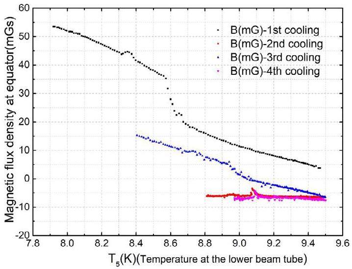
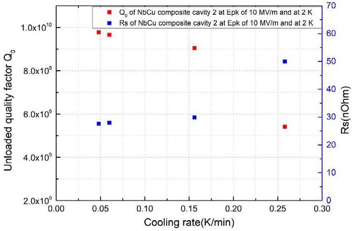
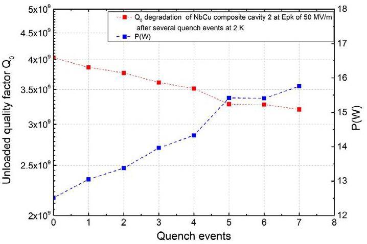
Figure 7 depicts the Q0 degradation and the corresponding power dissipation of the cavity 2 observed after several quenching events at 2 K. As evident, the Q0 degradation tended to saturate after multiple quenches subjected to the cavity, which is consistent with the earlier measurement reported by other researchers [40, 41]. The origin of Q0 degradation, attributed to the trapping of the magnetic flux generated by the thermal current during the quenching process, was clearly demonstrated in [40]. The number of trapped vortices in the Nb wall of the cavity after multiple quench events can be estimated by dividing the increase in power loss after quench events by the power dissipated by a single vortex. The power dissipated by a single vortex is expressed as Eq. (1) [42]:
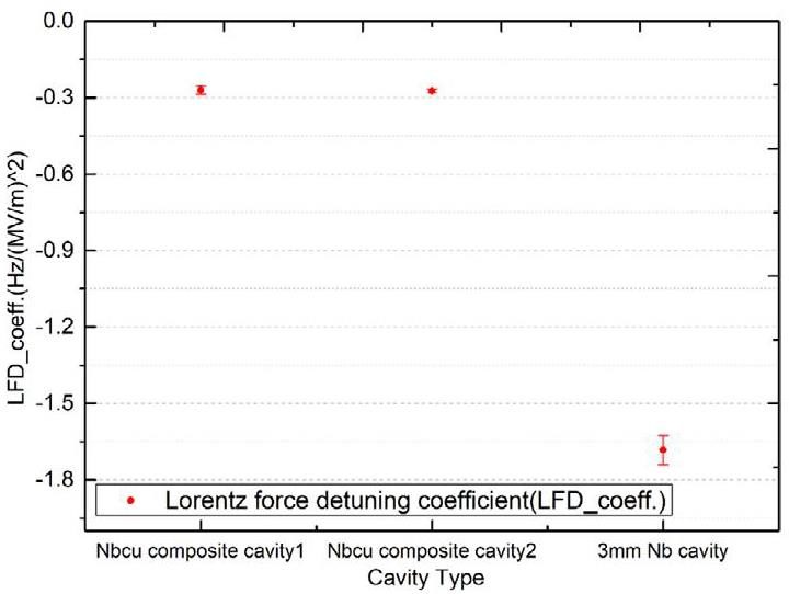
The pursuit of high mechanical stability is a key objective in the development of the Cu-Nb composite cavities. Therefore, the mechanical stability of the developed Cu-Nb composite cavities with respect to the Lorentz force detuning (LFD) coefficient and frequency detuning against He pressure fluctuation df/dp was measured and compared with the corresponding values of a 3 mm 1.3 GHz single-cell bulk Nb cavity tested in the same experiment. The LFD coefficient of bulk Nb cavity was more than six times higher than those of the two Cu-Nb composite cavities, as depicted in Fig. 8. The df/dp values of the cavity 2 and the bulk Nb cavity were ~ -17 Hz/mbar and ~ -106 Hz/mbar, respectively. This confirmed the enhanced mechanical stability of the Cu-Nb composite cavities.
Cu-Nb composite cavity made by electroplating Cu onto the bulk Nb cavities
In December 2020, we initiated the development and research of Cu-Nb composite cavities using the back-coating of Cu on the outer surface of a bulk Nb cavity by electroplating technology in collaboration with Ruiyuan Machinery Equipment Co., LTD at Lanzhou to avoid the problem of unreliable welding of the confronting Nb ends of the Cu-Nb composite sheets. By employing the traditional manufacturing method of bulk Nb cavities, that is, deep drawing, trimming, and electron beam welding of bulk Nb parts, etc., the superconducting RF performance of the Cu-Nb composite cavity is guaranteed.
Development of the cavity
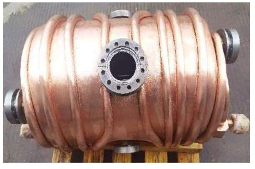
A Cu-Nb composite half-wave resonator labeled as the HWR030 NbCu composite cavity, with a frequency of 325 MHz and an optimal beta of 0.30, was fabricated, as shown in Fig. 9. Table 2 lists the RF parameters for the cavity. The fabrication procedure was as follows. (1) The bulk Nb cavity made of 3 mm thick high-purity Nb sheets (RRR > 300) was manufactured employing the traditional method, including deep drawing, trimming, cleaning of the cavity parts, and electron beam welding of the parts together. (2) The cavity outer surface was treated by sand blasting with 60 mesh fine sand and high-purity water cleaning in preparation for the subsequent electroplating process. The cavity was sealed with stainless steel flanges in this step. (3) A silver (Ag) layer of ~ 5 μm and a Cu layer of ~ 10 μm were electroplated sequentially on the processed outer surface of the cavity. After electroplating, the cavity underwent high-purity water cleaning, drying, and furnace processing at 850 ℃ for 70 mins under a vacuum pressure of less than 1×10⁻³ Pa. During this process, the cavity was mounted in a stainless-steel box, and the cavity flanges were covered with Nb foil. (4) The cavity outer surface was sand blasted, and the final thick Cu layer of ~5 mm was electroplated in the Cu sulfate plating solution on the surface of the thin Cu layer. The electroplating process was divided into two steps. a) The initial Cu layer of ~ 2 mm thickness was electroplated using a pulsed power supply. b) Subsequently, the remaining Cu layer of ~ 3 mm thickness was plated using a DC power supply. (5) Finally, the outer surface the Cu-Nb cavity was machined. It took two months to complete steps (2)–(4) for the HWR030 NbCu composite cavity. During the Ag and Cu electroplating process, the inner volume of the cavity was filled with high-purity water to protect the inner surface of the cavity against pollution from the electroplating solution. In step (3), a thin layer of Ag was used to enhance the bonding strength and minimize the thermal resistance between Nb and Cu because Cu and Nb can be treated as nonmiscible [43], which was also proposed for sputtered Nb thin films on Cu substrate superconducting cavities [44]]. Note that a Cu cooling pipe with an inner diameter of 10 mm was also arranged to study liquid He forced flow cooling for the cavity in another study.
| Parameters | Value |
|---|---|
| Frequency (MHz) | 325 |
| Beta | 0.3 |
| Epk/Eacc | 4.2 |
| Bpk/Eacc (mT/MV/m) | 6.9 |
| G (Ohm) | 97.43 |
| R/Q (Ohm) | 248.7 |
Cryogenic test results
In our study, cryogenic RF tests were conducted before and after Cu plating of the HWR030 cavity at both 4.2 K and 2 K, and the cavity was immersed in liquid He during the tests. Before testing the bulk Nb cavity, the following surface processing steps were applied: ~ 150 μm material removal by BCP using an acid mixture with a density of ~ 1.5 kg/L containing HF (40% wt.), HNO3 (65–68% wt.) and H3PO4 (85% wt.) with a volume ratio of 1:1:2 at a temperature below 12 ℃, and vacuum furnace outgassing at 600 ℃ for 10 hours, followed by an additional ~ 30 μm material removal by BCP, high-pressure rinsing, and baking at 120 ℃ for 48 hours in a clean room. Surface processing of the HWR030 Cu-Nb cavity involved ~ 30 μm material removal by BCP, vacuum furnace processing at 600 ℃ for 10 hours for stress relief, and another ~ 30 μm material removal by BCP, high-pressure rinsing, and baking at 120 ℃ for 48 hours in a clean room. Considering the test results of the 1.3 GHz Nb composite cavity, which indicated that a low cooling rate at the Tc crossing of Nb was preferable for achieving a high Q0 for the Cu-Nb composite cavity, the cooling rate of the HWR030 Cu-Nb composite cavity was carefully controlled. A cooling rate of 0.35 K/min was obtained at temperatures ranging within 10.25–8.25 K. Consequently, the magnetic flux density recorded on the outer surface of the cavity, including the background magnetic field and thermal-current-induced magnetic field, was less than 10 mGs during the Tc crossing of Nb.
Figure 10 shows the RF test results for the HWR030 cavity before and after Cu electroplating. The performance of the bulk Nb cavity was limited by field emission, with the peak electric field Epk reaching ~ 46 MV/m at both 4.2 K and 2 K. Approximately 30% Q0 degradation was observed after Cu electroplating during the tests at 4.2 K, which might be attributed to the additional surface processing of the Cu-Nb composite cavity and/or the existence of the 5 mm thick Cu layer between the 3 mm Nb and the liquid He. Considering that the Cu/HeII Kapitza resistance is in the same range as that of the Nb/HeII interface [44], the introduction of the Cu layer increases the overall thermal resistance of the cavity wall. Further studies are required to understand the Q0 degradation. Despite the thick Cu layer deposition on the HWR030 cavity, a remarkably high Epk of ~ 88.8 MV/m, corresponding to Bpk of ~ 145.9 mT, was still achieved at 2 K. Q0 at Epk of 88.8 MV/m at 2 K exceeded 1×10¹⁰ and the corresponding surface resistance Rs is 9.6 nΩ. No Q0 slope was observed up to Epk of ~ 88.8 MV/m at 2 K for the HWR030 NbCu composite cavity.
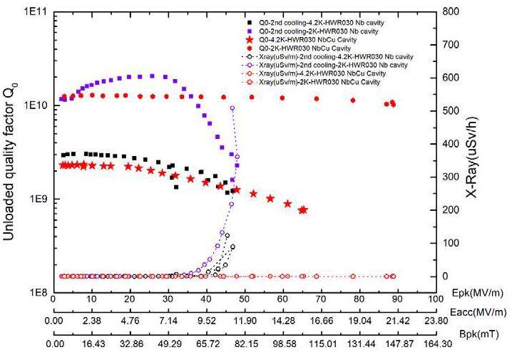
In the sample study, Cu cut from the outer surface of the cavity and subjected to heat treatment at 600 ℃ for 10 hours exhibited an RRR of ~ 56 and thermal conductivity of ~ 300 W/(m·K) at 4.2 K. As reported in [45], electroplating Cu with a thermal conductivity exceeding 1000 W/(m·K) at 4.2 K can be achieved using pulsed plating and subsequent heat treatment. Therefore, Cu-Nb composite cavities fabricated by electroplating Cu on the bulk Nb cavity have significant potential for achieving high thermal stability against thermal breakdown triggered by defects in the SRF cavities.
The mechanical performance with respect to df/dp and LFD coefficient of the HWR030 cavity were measured before and after back-coating with Cu. df/dp was decreased from ~ 48.27 Hz/mbar to ~ 15.51 Hz/mbar. In addition, an LFD coefficient of ~ 1.73 Hz/(MV/m)2 was obtained and compared with the value of ~ 7.58 Hz/(MV/m)2 for the bulk Nb cavity. This indicates that back-coating Cu on the outer surface of a bulk Nb cavity is an effective method for enhancing the mechanical stability of the cavity, even when the cavity is immersed in liquid He. The mechanical stability can be further increased as the cavity design aims to maintain a working temperature of 4.2 K, with only a portion of the cavity's outer surface in direct contact with liquid He.
Summary and outlook
Cu–Nb composite superconducting cavities have excellent potential for high thermal and mechanical stability. They can exploit the high-gradient surface processing recipes developed for bulk Nb cavities, high thermal conductivity of the thick Cu layer (~ 400 W/(m·K) at 4.2 K), and structural rigidity. Several studies have been conducted on the Cu-Nb composite cavities to achieve high mechanical stability and/or cost-effective mass production. However, further investigation is essential to explore its engineering applications with a high accelerating gradient and Q0 using reliable technical methods, particularly for low-beta SRF cavities.
The stringent reliability requirements of the superconducting linac for the CiADS project and the fact that the operational instability of the Chinese ADS Front-end Demo linac (CAFe) was significantly influenced by the SRF cavity system are considered. Therefore, both Cu-Nb composite cavities based on Cu-Nb composite sheets and the electroplating Cu approach are being explored at the IMP. Our research confirmed that the Cu-Nb composite cavities, even when immersed in liquid He, exhibited high mechanical stability in terms of the LFD coefficient and df/dp. Further enhancement in the mechanical stability is anticipated, as the cavity design facilitates the maintenance of working temperatures at 4.2 K or 2 K, with only a portion of the cavity's outer surface in contact with liquid He.
The investigation of 1.3 GHz single-cell Cu-Nb composite cavities indicated that the wavy structure at the Cu-Nb interface introduced by the explosive bonding technique can be eliminated by the HIP technique, which enhanced the reliability of welding between composite parts. The magnetic flux density generated and trapped during the Tc crossing of Nb in cooldown process, which is attributed to the Seebeck effect of the Cu-Nb bimetallic structure, degraded the RF performance of the cavities. The saturation of the surface resistance Rs related to the magnetic flux trapping was observed by decreasing the cooling rate during the Tc crossing of Nb. Therefore, slow cooling is preferred to obtain high-performance Cu-Nb composite cavities. However, the Q0 of the 1.3 GHz Cu-Nb composite cavities was less than 1×10¹⁰ at 2 K, which may be attributed to Cu evaporation and deposition in the welding seam of Nb. The Q0 degradation also tended to saturate after several quenches subjected to the cavity. Further studies on the low Q0 problem should be conducted by optimizing the manufacturing conditions for the Cu-Nb composite sheets, welding conditions, and the surface process of the cavity. For cavities made of Cu-Nb composite sheets and fabricated using the traditional manufacturing method for bulk Nb cavities, it is essential to develop a reliable technique for patching up the groove in the welding seam area between the Cu-Nb composite parts with Cu, as the bonding condition between Nb and Cu will affect the RF heat transfer efficiency of the Cu-Nb composite cavity for the cooling medium.
To the authors' knowledge, this study is the first to report the plating of Cu on the outer surface of a low-beta bulk Nb cavity (HWR030) via electroplating technology to avoid possible Q0 degradation related to the welding of the Cu-Nb composite parts. An Ag buffer layer was used to enhance the bonding strength and minimize the thermal resistance between the Nb substrate and the Cu layer. Although the Nb and Cu layers were 3 mm and 5 mm in thickness, respectively, a remarkably high Epk of ~ 88.8 MV/m, corresponding to the Bpk of ~ 145.9 mT, was still achieved at 2 K. the Q0 at Epk of 88.8 MV/m exceeded 1×10¹⁰, which corresponds to the surface resistance Rs of 9.6 nΩ. Despite approximately 30% Q0 degradation after Cu electroplating, the electroplating technology still exhibits excellent potential for manufacturing the Cu-Nb composite cavities that operate at a high accelerating gradient Eacc with high thermal and mechanical stability.
For the engineering application of a specific Cu-Nb composite cavity type, the frequency shift of the Cu-Nb composite cavity during heat treatment must be controlled because of the different thermal expansion coefficients of Cu and Nb. The Cu and Nb structures (i.e., the thickness ratio of the Cu layer to the Nb layer) and cooling scheme of the cavity must be carefully designed, particularly in the beam tube region, to render the beam tube region tunable for frequency tuning, minimize magnetic flux generation and trapping during quench events, and ensure efficient RF heat transfer to the cooling medium. These considerations contribute to achieving cavities with high thermal and mechanical stability.
Nitrogen and argon doping of niobium for superconducting radio frequency cavities: a pathway to highly efficient accelerating structures
. Supercond. Sci. Technol. 26,Successful Nitrogen Doping of 1.3GHz Single Cell Superconducting Radio-Frequency Cavities
. Chinese Phys. Lett. 35,Nitrogen doping with dual- vacuum furnace at IHEP
. Nucl. Instrum. Meth. A 993,Nitrogen doping/infusion of 650 MHz cavities for CEPC
. Nucl. Sci. Tech. 32, 45 (2021). https://doi.org/10.1007/s41365-021-00881-3Accelerating gradient improvement in nitrogen-doped superconducting radio-frequency cavities for SHINE
. Nucl. Instrum. Meth. A 1057,Unprecedented quality factors at accelerating gradients up to 45 MVm-1 in niobium superconducting resonators via low-temperature nitrogen infusion
. Supercond. Sci. Technol. 30,The effect of nitrogen infusion on a 162.5 MHz low beta superconducting HWR cavity
. Nucl. Instrum. Meth. A 937, 21-25 (2019). https://doi.org/10.1016/j.nima.2019.04.087Medium-temperature baking of 1.3 GHz superconducting radio frequency single-cell cavity
. Radiat. Detect. Technol. Methods 4, 507-512 (2020). https://doi.org/10.1007/s41605-020-00208-7Medium-temperature furnace baking of 1.3 GHz 9-cell superconducting cavities at IHEP
. Supercond. Sci. Technol. 34,Quality Factor Enhancement of 650 MHz Superconducting Radio-Frequency Cavity for CEPC
. Appl. Sci. 12, 546 (2022). https://doi.org/10.3390/app12020546Ultrahigh accelerating gradient and quality factor of CEPC 650 MHz superconducting radio-frequency cavity
. Nucl. Sci. Tech. 33, 125 (2022). https://doi.org/10.1007/s41365-022-01109-8Surface resistance effects of medium temperature baking of buffered chemical polished 1.3 GHz nine-cell large-grain cavities
. Supercond. Sci. Technol. 36,In-situ plasma processing to increase the accelerating gradients of superconducting radio-frequency cavities
. Nucl. Instrum. Methods Phys. Res. A 812, 50-59 (2016). https://doi.org/10.1016/j.nima.2015.12.043In-situ plasma cleaning to decrease the field emission effect of half-wave superconducting radio-frequency cavities
. Nucl. Instrum. Meth. A 905, 61-70 (2018). https://doi.org/10.1016/j.nima.2018.07.039Superconducting Accelerating Cavity Pressure Sensitivity Analysis and Stiffening
. in Proceedings of LINAC2014,Commissioning of China ADS demo Linac and baseline design of CiADS project
. J. Phys.: Conf. Ser. 1401,Overview and SRF Requirements of CiADS Project, invited talk
, in Proceedings of SRF2019,An approach to characterize Lorentz force transfer function for superconducting cavities
. Nucl. Instrum. Meth. A 1012,In situ mitigation strategies for field emission-induced cavity faults using low-level radiofrequency system
. Nucl. Sci. Tech. 33, 140 (2022). https://doi.org/10.1007/s41365-022-01125-8Precise calibration of cavity forward and reflected signals using low-level radio-frequency system
. Nucl. Sci. Tech. 33, 4 (2022). https://doi.org/10.1007/s41365-022-00985-4Niobium films for superconducting accelerating cavities
. Appl. Phys. Lett. 45, 583-584 (1984). https://doi.org/10.1063/1.9528920 Years of experience with the Nb/Cu technology for superconducting cavities and perspectives for future developments
. Phys. C 441, 95-101 (2006). https://doi.org/10.1016/j.physc.2006.03.044Nb Sputtered Quarter Wave Resonators for the HIE-ISOLDE
. in Proceedings of SRF2013,Performance of ALPI new medium beta resonators
. in Proceedings of HIAT 2012,Study of the influence of the manufacturing process and thermal cycling on the RF performance of 1.3 GHz Nb/Cu SRF cavities
. in the 10th International Workshop on Thin Films and New Ideas for Pushing the Limits of RF Superconductivity,Results of the R&D RF Testing Campaign of 1.3 GHz Nb/Cu Cavities
. in Proceedings of SRF2023,Report of meetings of Thin Film working group and Thin Film workshop
. in TTC Meeting 2022,First three years operational experience with the JAERI tandem-booster
. in Proceedings of the 1997 Workshop on RF superconductivity,R&D of Nb/Cu Clad Seamless Cavities at KEK
. in Proceedings of the 10th Workshop on RF Superconductivity,SRF Cavity Stiffening by Thermal Spraying
. in Proceedings of EPAC 2000,Multi-metallic conduction cooled superconducting radio-frequency cavity with high thermal stability
. Supercond. Sci. Technol. 33,Status and Challenges of Nb/Cu SRF Cavities for Superconducting Linac, Invited talk
. in the 31st International Linear Accelerator Conference,Progress and Operation Experience at CAFe, invited talk
. in Proceedings of SRF2021,Ultra-high quality factors in superconducting niobium cavities in ambient magnetic fields up to 190 mG
. Appl. Phys. Lett. 105,Magnetic flux studies in horizontally cooled elliptical superconducting cavities
. J. Appl. Phys. 118,Dependence of trapped-flux-induced surface resistance of a large-grain Nb superconducting radio-frequency cavity on spatial temperature gradient during cooldown through Tc
. Phys. Rev. Accel. Beams 19,Impact of cool-down conditions at Tc on the superconducting rf cavity quality factor
. Phys. Rev. Spec. TOP-AC. 16,MAGNETIC FLUX GENERATED BY THERMAL CURRENT IN CEBAF 5-CELL CAVITY SYSTEM
. in Proceedings of the 29th Linear Accelerator Conference,Effect of coodown and residual magnetic field on the performance of niobium-copper clad superconducting radio-frequency cavity
. Supercond. Sci. Technol. 31,Hydroforming of NbCu Clad Cavities at DESY
. in Proceedings of the 10th Workshop on RF Superconductivity,Effect of vortex hotspots on the radio-frequency surface resistance of superconductors
. Phys. Rev. B 87,Cu-Nb Bull
. Alloy Phase Diagrams 2, 455 (1982).Thermal contact resistance at NbCu interface as a limiting factor for sputtered thin film RF superconducting Cavities
. Supercond. Sci. Technol. 29,Electrodeposition of copper applied to the manufacture of seamless SRF cavities
. Phys.Rev.Accel.Beams 24,The authors declare that they have no competing interests.

