Introduction
High-voltage drivers are used to drive power metal-oxide-semiconductor field-effect transistors (MOSFETs), which are widely applied in power systems, motor drive systems, and radar transceivers of satellites [1-4]. However, radiation in aerospace can reduce chip performance in high-voltage drivers, occasionally causing total system failure.
The total ionizing dose (TID) significantly affects MOSFET performance. Furthermore, the chips used in high-voltage applications require a MOSFET with a thick gate oxide to ensure a high gate-to-source voltage (VGS). However, the number of trap holes generated in response to the TID effect increases with the thickness of the gate oxide. Consequently, in conventional chips, the threshold voltage VTH of an n-type MOSFET (NMOS) may drop below 0 V after TID irradiation, leading to the inadvertent activation of the system despite the absence of an additional gate bias [5-8].
The single-event effect (SEE) occurs when high-energy protons and heavy ions in space collide with the sensitive nodes of a microelectronic device, generating an additional charge through ionization. This charge alters the logic state of a device, leading to functional interference or even device failure [9-11]. Conventional high-voltage drivers are vulnerable to SEE. Moreover, during SEE episodes, the parasitic bipolar junction transistor (BJT) in high-voltage MOSFETs is more susceptible to unwanted turn-ons than that in low-voltage MOSFETs [12].
Several new strategies have been developed for fabricating radiation-hardened MOSFET chips [13]. To improve TID tolerance, Lei et al. proposed that the replacement of the typical high-voltage NMOS transistor in the output circuit of a driver with an n-p-n transistor to avoid performance degradation after TID irradiation [14]. However, the SEE or TID tolerance of the chip during the high-voltage input stage was not examined. Aubuchon et al. explored a new production method for MOSFET gate oxides that changed the temperature, environment, and steps of the oxidation process to reduce the oxide defect charge induced by TID irradiation. The resulting MOSFETs exhibited higher TID tolerance than those produced through conventional processes [15, 16]. However, the process flow cannot be integrated into conventional commercial processes, which significantly limits the application of this strategy.
Similarly, researchers have attempted to improve SEE tolerance by developing single-event-hardened devices to reduce the possibility of parasitic BJT activation. For example, Dodd et al. proposed a method that involved the addition of a buried P+ layer under the source of the MOSFET. They employed a heavily doped body contact and incorporated a heavily doped P+-buried layer underneath the source [17]. However, this P+ buried layer required a unique fabrication method that did not align with traditional bipolar complementary metal oxide semiconductor (CMOS)–double-diffused metal oxide semiconductor (DMOS) (BCD) processes. Previously, we developed a layout optimization strategy that increased the length of the n-type drift region in the n-channel lateral double-diffused metal-oxide-semiconductor field-effect transistor (NLDMOS) to improve the SEE tolerance of the device. This method reduced the amplification of the parasitic BJT and electric field intensity of the drift region at the same voltage by increasing the length of the drift region, which increased the chip area [18]. However, the aforementioned studies primarily focused on the development of radiation-tolerant output circuits, and few studies on radiation-tolerant methods that target input circuits have been performed.
In this paper, we present a comparator input unit and level-shift unit that increase the TID tolerance of a MOSFET driver and a novel DSS ring structure that increases its SEE tolerance. Notably, p-type MOSFETs (PMOS) exhibit better TID tolerance than NMOS. Hence, we developed a comparator using a high-voltage PMOS with a thick gate oxide and a low-voltage NMOS with a thin gate oxide to replace the high-voltage thick-gate-oxide NMOS present in conventional input circuits. Our experiments indicated that the functional parameters of the chips containing this novel comparator remained normal even at a TID of 300 krad(Si), whereas those of the unreinforced chips were altered at a lower TID of 100 krad(Si). We also conducted simulations to assess the SEE tolerance of two types of NLDMOS devices featuring different source and drain locations, which were fabricated based on the ring-gate structure required for TID tolerance. The results indicated that the NLDMOS with a DSS structure exhibited better SEE tolerance than that with an SSD structure. Subsequently, the experimental results confirmed that the chip with the novel DSS structure withstood an SEE greater than 81.8 MeV cm2mg-1. Finally, we identified the sensitive regions of the chip under single-particle irradiation, providing an intuitive and effective strategy for positioning other sensitive regions under these conditions.
Characteristics of conventional (unreinforced) high-voltage drivers
The schematic of a typical unreinforced high-voltage driver circuit consisting of an input unit, a switching manager, a gate driver, and an output unit is presented in Fig. 1(a). To ensure that both the input and output voltages reached 20 V, NMOS and PMOS with 1000 Å-thick gate oxides were used in the input and output units of a typical high-voltage driver circuit because the gate oxide thickness is associated with VGS.
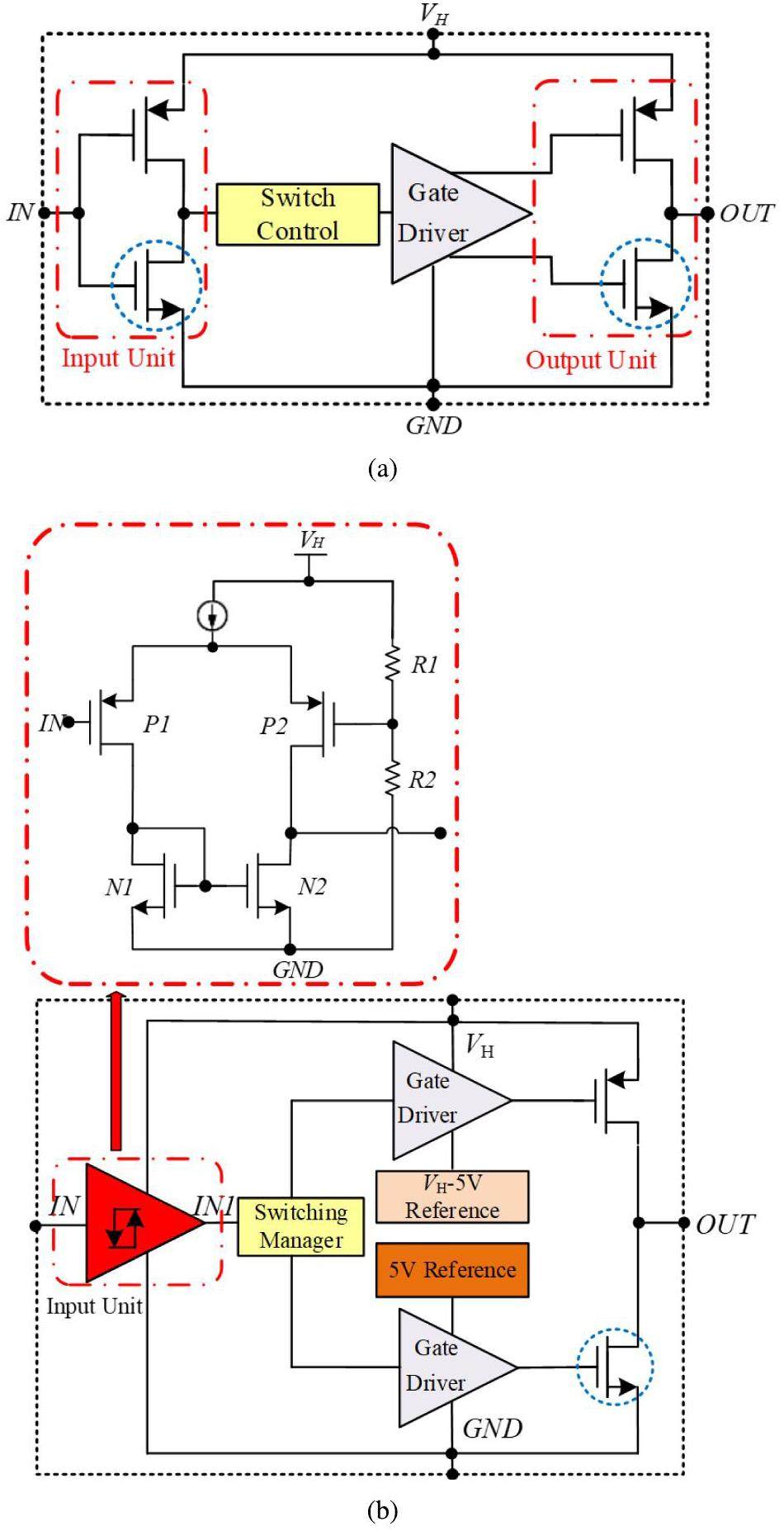
TID irradiation increases leakage currents [19, 20] primarily because of the parasitic currents between the drain and source of the NMOS, which are induced by the exit of the field oxide layer under TID irradiation. Moreover, a thick oxide layer results in a more severe TID effect, and the VTH shift induced by the TID is proportional to the square of the oxide thickness. Therefore, the fixed charge density produced by the TID effect can increase the gate-to-source leakage current in the thick-gate oxide NMOS devices. This results in a negative VTH shift, rendering the NMOS vulnerable to unwanted turn-on. VTH can shift below 0 V after TID irradiation, which impairs driver function, particularly in high-voltage thick-gate-oxide devices. Furthermore, CMOS circuits are susceptible to latch-up owing to attacks by high-energy particles, which can cause unwanted parasitic BJT device turn-on in a thyristor-like mode [21, 22]. The energy transferred from the incident particles produces electron-hole pairs (EHPs), which alter the electric field distribution of the epitaxial layer and activate the parasitic BJTs, eventually triggering single-event burnout (SEB). The drain current of the NMOS continues to increase until burnout occurs. Hence, the TID and SEB tolerances of typical high-voltage drivers are extremely low. Therefore, the structure shown in Fig. 1(a) cannot resist TID and SEE irradiation and the chip exhibits impaired function or damage after irradiation in space.
Design of a radiation-tolerant high-voltage driver
TID-tolerant design with a comparator input unit
The oxide trap charge produced by the TID in the gate oxide layer of NMOS devices causes a negative shift in VTH. Hence, the high-voltage thick-gate-oxide NMOS experiences a more severe TID effect. The isolation oxide is instrumental in the TID response of the device, because its thickness is much greater than that of the gate oxide. Here, the number of charges increases with the ionizing dose, which results in substrate depletion or even inversion. Thus, the device becomes depleted and cannot be shut off normally. Owing to the extremely low TID tolerance of high-voltage NMOS, the design of the input circuit must be optimized. As described earlier, the reduced VTH of PMOS prevents the device from continuously remaining on. Hence, we designed a comparator comprising high-voltage PMOS and low-voltage NMOS devices (Fig. 1(b)). As this comparator design lacks a high-voltage NMOS, which is most susceptible to TID irradiation, it exhibits enhanced TID tolerance.
A high-voltage PMOS named P1 with a 1000 Å-thick gate oxide was used as the input device in the input unit of the comparator structure (Fig. 1(b)). Because the NMOS is located on the P-type substrate, the accumulated charge in the isolated oxide layer increases with the total dose. This accumulated charge can invert the substrate under the isolated oxide layer from P- to N-type, forming N-type channels and parasitic NMOS transistors. The parasitic NMOS was parallel to the main transistor and significantly increased the turn-off leakage current. However, because the PMOS was located in the N-well, the trap charges generated in the isolated oxide layer after TID irradiation did not cause N-type interface inversion. Hence, the leakage current generated by TID irradiation in the PMOS was minimal [23-25]. Consequently, PMOS performed better than NMOS against TID irradiation.
The resistances R1 and R2 provide the reference voltage for the comparator. VGS of the thick-gate oxide PMOS device was above 24 V, satisfying the maximum input requirement of 20 V. The sources of the two thick-gate oxide PMOS devices (P1 and P2) were connected to a high voltage VH, which was equal to the supply voltage of 20 V in this circuit. The gate of P1 was used as the input of the comparator, while the drain of P1 was connected to the drain of the NMOS with a 200 Å thin gate oxide (N1). The drain of P2 was connected to the drain of the NMOS with a 200 Å thin gate oxide (N2), and the drain of N1 was connected to the gate. The sources of N1 and N2 were connected to the GND. When the input voltage was lower than 0.8 V, VGS(P1) was greater than VGS(P2), and the current generated on VH primarily flowed through P1 and N1. Hence, P1, N1, and N2 were on; the output voltage IN1 was close to GND; and the output was low. The simulation analysis indicated that the output voltage IN1 was approximately 1 mV under these conditions. In contrast, when the input voltage was higher than 2.4 V, VGS(P1) was lower than VGS(P1), and the current generated from VH primarily flowed through P2 and N2. P2 was open; hence, output voltage IN1 was close to VH. Thus, the output was high, and the simulation analysis indicated that the output voltage IN1 under these conditions was approximately 4 V.
Meanwhile, the VTH shift in the PMOS after TID irradiation did not affect the function of the comparator. In the comparator, the irradiation performance degradations of the high-voltage PMOS (P1 and P2) and low-voltage NMOS (N1 and N2) devices were synchronized. This eliminated the influence of the VTH shift of the single NMOS, preventing alterations in the current distribution of the input structure and output voltage IN1 of the comparator after irradiation. Therefore, this structure improves the TID tolerance of high-voltage input structures.
For the output circuit, we employed a previously reported level-shift unit method to increase the TID tolerance [19] (Fig. 1(b)). The level-shift unit in this radiation-resistant circuit generated references of 5 V and VH-5 V. The 5 V and VH-5 V references were applied to the gates of the NMOS and PMOS, respectively. Hence, the gate voltage of the MOSFET in this circuit was reduced to 5 V, enabling the adoption of a thin-gate-oxide device. Meanwhile, an LDMOS with a VGS of +5 V and drain-source voltage (VDS) of 20 V was used as the output device to achieve an output voltage of 20 V along with good TID tolerance. Overall, this design provided higher radiation tolerance to the driver by eliminating the use of the TID-sensitive thick-gate-oxide NMOS through the design of the harden schematic.
SEE-tolerance design using a novel NLDMOS structure
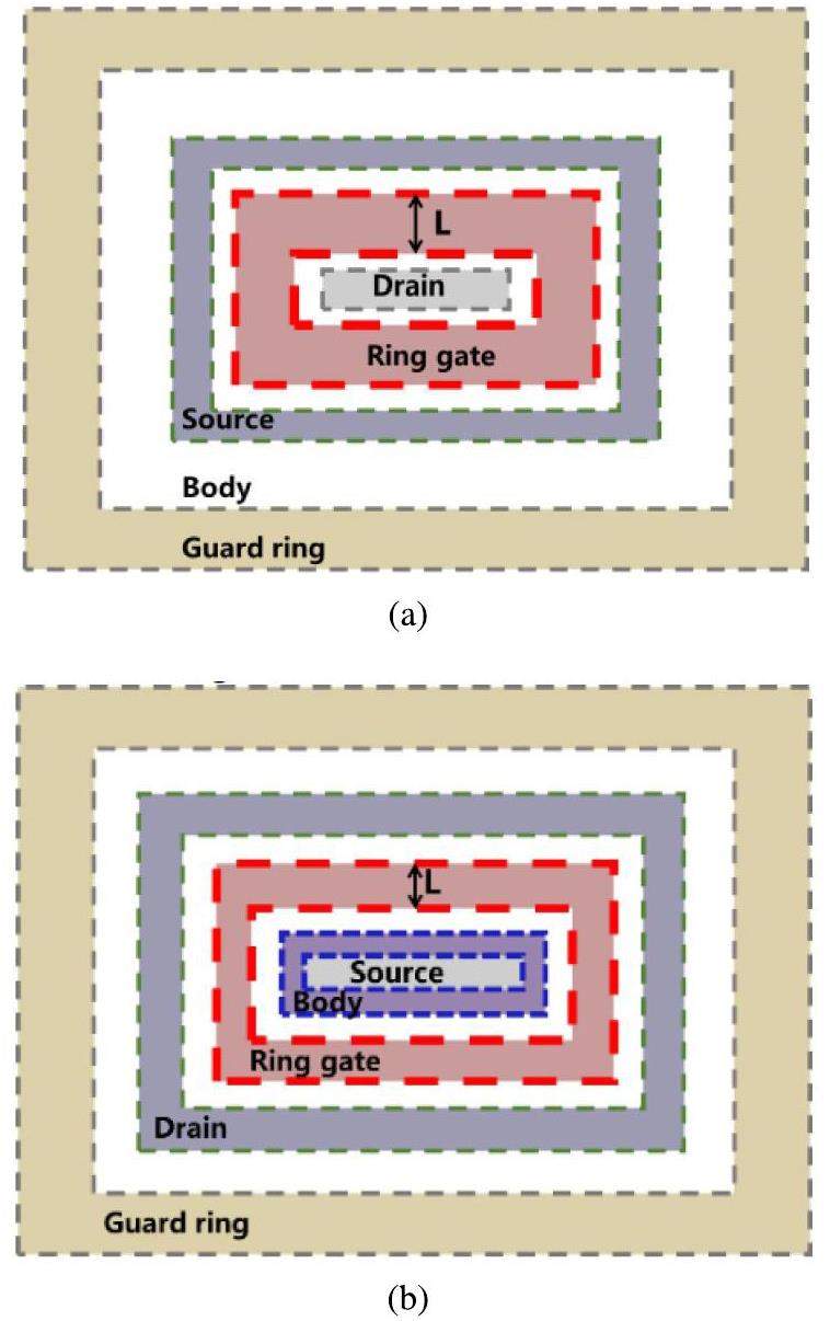
To reduce the single-particle-induced current in MOSFET, both SSD and DSS configurations were designed based on an enclosed-layout transistor (ELT) structure, as shown in Fig. 2(a) and (b), respectively. As shown in Fig. 2, the body region surrounding the source in the DSS structure is smaller than that in the SSD structure. Hence, the P-region area of the parasitic NPN transistor is smaller. Consequently, the amount of charge triggered following the single-particle irradiation is less than that triggered in the device with the SSD structure, leading to a lower probability of unwanted parasitic BJT turn-on. Therefore, the DSS structure provides stronger SEE tolerance than the SSD structure.
Design of the overall layout of the high-voltage radiation-tolerant driver
The method proposed to increase the radiation tolerance in this study is based on a commercial process. Importantly, it does not involve any modifications to the process flow because the layout is adjusted without altering basic processes or manufacturing steps employed for fabricating common devices. By optimizing the chip layout, as mentioned in the previous section, the leakage current generated by the TID effect and the current concentration effect generated by the SEE can be mitigated. This is because MOSFETs have an ELT gate layout that eliminates the leakage channel created between the source and drain of the edge of the field oxide caused by the TID effect. Additionally, adjusting the positions of the source and drain in MOSFETs with an ELT gate layout can reduce the current induced via single-particle irradiation.
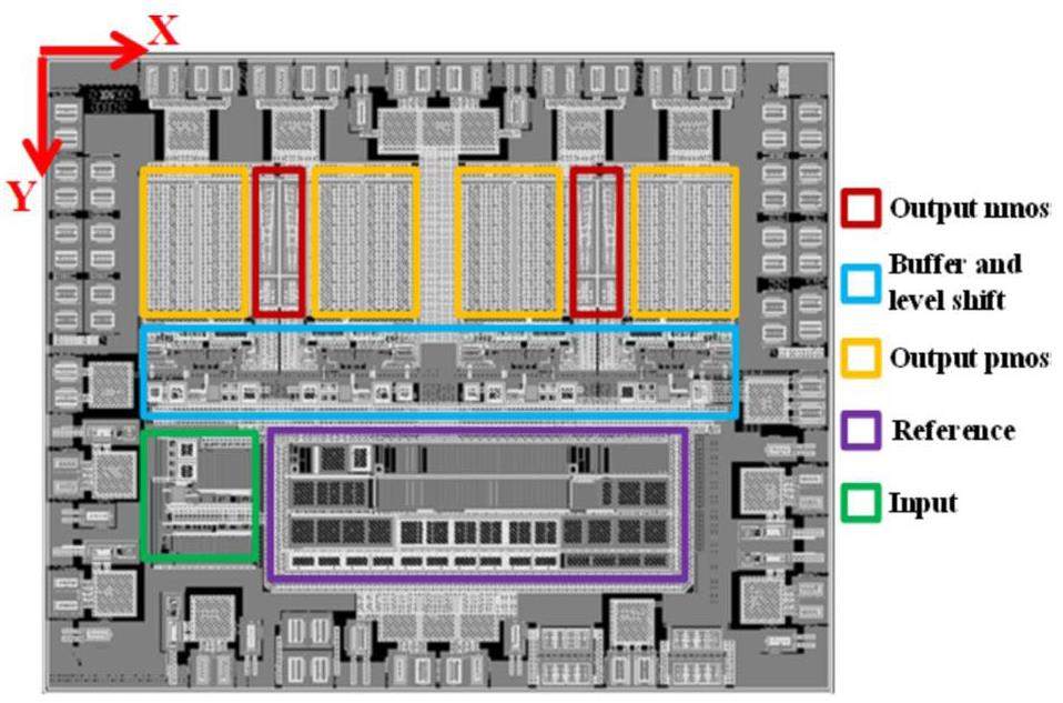
The overall layout of the high-voltage driver was symmetrical (Fig. 3). Four independent driver channels were integrated into one chip to enable multichannel driving. All four channels shared an input stage and a power supply unit. In the layout, the input device was next to the input port; the reference, buffer, and level-shift unit were at the center of the overall layout to provide a bias voltage or input to other devices. The output device was next to the output port, and the output NMOS and PMOS devices were symmetrically distributed such that the PMOS of the two channels shared an N-well, which reduced the layout area. A three-layer wiring design was adopted to reduce the layout area and increase the degree of integration. Additionally, electrostatic discharge (ESD) protection devices were installed near all the input/output (I/O) and power ports to improve the ESD tolerance of the driver. The NMOS in the layout adopted two structures based on the SSD and DSS configurations.
Irradiation experiments
Four types of chips were fabricated using a commercial 0.35-μm BCD process, as listed in Table 1. A common commercial process provided the high-voltage devices required for this design, and the fabrication of these chips was cost-effective and suitable for this application. The Type 1 and Type 2 chips used a typical input structure with different NMOS layouts in the SSD and DSS configurations, while, the Type 3 and Type 4 chips used a comparator input structure with different NMOS layouts in the SSD and DSS configurations. The area of all the chips was 3.3 mm × 2.5 mm because this design was compatible with the package structure of the chips and test system for the subsequent experiments. Before the irradiation experiment, the basic functional parameters of the four chips were tested. The results indicated that the basic functional parameters of all the four chips satisfied the design index requirements. All the four chips exhibited normal output waveforms corresponding to a high-frequency input signal of 40 MHz. In addition, no significant differences in the output waveforms of the chips were observed, indicating that the input structure and NMOS layout did not significantly affect the high-frequency and high-voltage output performances of the chips. Nevertheless, slight differences in the tested and emulational output waveforms were observed owing to the influence of the parasitic loads generated by the test system. Subsequently, TID and SEE irradiation experiments were performed to evaluate the performances of the four chips, as described below.
| Device | Input structure | NMOS layout |
|---|---|---|
| Type 1 | Typical structure | SSD |
| Type 2 | Typical structure | DSS |
| Type 3 | Comparator structure | SSD |
| Type 4 | Comparator structure | DSS |
TID experiments
The TID experiments were conducted at the Xinjiang Technical Institute of Physics and Chemistry, Chinese Academy of Sciences, China. Co-60 was used as the radiation source, and three different irradiation doses, i.e., 100 krad(Si), 200 krad(Si), and 300 krad(Si), with a dose rate of 50rad(Si)s-1, were selected. A 20 V program-controlled power supply was used to supply power to the test samples, and a signal source was used to provide a 40 MHz high-frequency input signal. A customized automatic test system was employed to test the key electrical parameters of the chips (drain current (Id), input low voltage (VIL), and supply current (ISL)) before and after irradiation to observe the effect of TID [26-28]. The devices were tested 20 min after irradiation to reduce the annealing effect.
The basic functional parameters of the high-voltage driver, that is, Id, VIL, ISL, rise time (Tr), and fall time (Tf), were evaluated before and after TID irradiation (Fig. 4). Here VIL denotes the tested low voltage at which the input unit functions normally; ISL represents the supply current at the input voltage VIN= 0 V; Tr represents the rise time of the output waveform when the input is a 100 kHz square wave; and Tf represents the fall time of the output waveform with the same input. The test data showed that the VIL values of the two hardened devices (types 3 and 4) were above 0.8 V after 100 krad(Si), 200 krad(Si), and 300 krad(Si) irradiation.
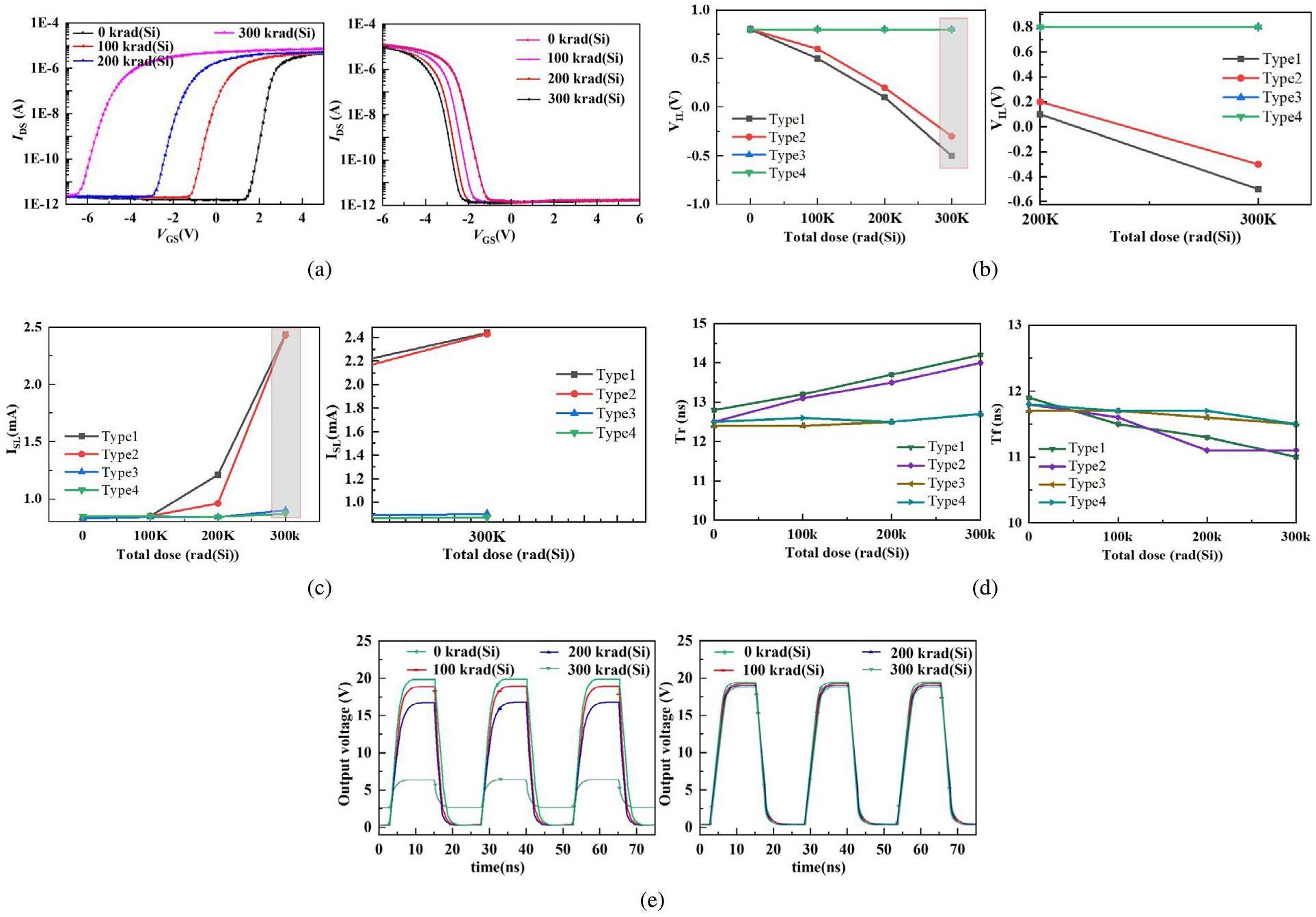
However, the VIL of the two unhardened devices (types 1 and 2) shifted to 0.5 V and 0.6 V after 100 krad(Si) irradiation and to 0.1 V and 0.2 V after 200 krad(Si) irradiation, respectively. Thus, the driver provided a low output only when the input voltage was below 0.5 V and 0.6 V after 100 krad(Si) irradiation and below 0.1 V and 0.2 V after 200 krad(Si) irradiation. Additionally, the Tr of the two unhardened devices (types 1 and 2) shifted from 12.8 ns and 12.5 ns to 13.2 ns and 13.1 ns after 100 krad(Si) irradiation and to 13.3 ns and 13.5 ns after 200 krad(Si) irradiation, respectively. This was attributed to the increase in the absolute value of VTH of the PMOS after TID irradiation, indicating a decrease in its conduction capacity and a subsequent increase in the output rise time. Meanwhile, the Tf of the two unhardened devices (types 1 and 2) changed from 11.9 ns and 11.8 ns to 11.5 ns and 11.6 ns after 100 krad(Si) irradiation and to 11.3 ns and 11.1 ns after 200 krad(Si) irradiation, respectively. This is because the absolute value of VTH of the NMOS decreases after TID irradiation, increasing its conduction capacity and decreasing its output fall time. The trends of Tr and Tf are observed in the output waveforms shown in Fig. 4(e)).
The static noise margin (SNM) reflects the ability of the chip to withstand static noise and can be classified into low SNM (LSNM) and high SNM (HSNM). LSNM is equivalent to the voltage difference between VIL and GND, whereas HSNM is equivalent to the voltage difference between VIH and the power supply voltage. Here, the LSNMs of the Type 1 device were 0.5 V, 0.1 V, and -0.5 V after 100 krad(Si), 200 krad(Si), and 300 krad(Si) irradiation, respectively.
Furthermore, the VIL values of both unhardened devices (types 1 and 2) dropped below 0 V at a TID of 300 krad(Si)because VTH of the thick-gate-oxide NMOS shifted as the total dose increased, decreasing to below 0.8 V and 0 V after 100 krad(Si) and 300 krad(Si) irradiation, respectively. Thus, the thick-gate-oxide NMOS was turned on at VIL=0.8 V and VIL=0 V after 100 krad(Si) and 300 krad(Si) irradiation, respectively, causing the driver to constitutively stay on and behave abnormally. In addition, ISL increased from 0.85 mA before TID irradiation to 2.44 mA (Type 1) and 2.43 mA (Type 2) after 300 krad(Si). This is because certain devices inside the driver could not be turned off under these test conditions, thereby increasing the leakage current. In contrast, all tested VIL, ISL, Tr, and Tf values for the hardened Type 3 and Type 4 devices remained stable before and after TID irradiation.
The results presented in Fig. 4 suggest that the functional parameters of the two hardened devices with the novel comparator structure remained normal after 300 krad(Si) TID irradiation, which aligns with our proposed design. This suggests that the input high-voltage comparator composed of the thick-gate PMOS and thin-gate oxide NMOS exhibits improved TID tolerance, and the influence of the VTH shift and leakage current in the input high-voltage comparator following TID irradiation is significantly weaker than that in a typical high-voltage driver.
SEE experiments
Subsequently, we used TID-hardened Type 3 and Type 4 devices for the SEE experiments. These experiments were conducted at the Institute of Modern Physics, Chinese Academy of Sciences, using the heavy-ion research facility at Lanzhou (HIRFL), with different accelerating particles with a linear energy transfer (LET) ranging from 8 to 100 MeV cm2mg-1 [29-31].
Ti and Bi ions (LET = 81.8 MeV cm2mg-1 and 99.9 MeV cm2mg-1 and ion emission distances in Si =27.3 μm and 15.2 μm, respectively) were selected. The ions were almost vertically incident on the chips and the ion fluence was 10×107 cm-2. Heavy ions collide with semiconductor materials, creating an ionization path with high charge density and activating the parasitic BJT in the MOSFETs. The power supply voltage was 20 V. A square wave was adopted as the input signal to control the MOSFETs, and the driver input was programmed to be 0 V or 20 V. While increasing the ion dose from 0, the changes in the power supply current and output voltage were monitored at recording intervals of 1 s using an ammeter and oscilloscope, as single-particle irradiation typically induces a current pulse first. To ensure safety, the maximum probing power supply current was set to 100 mA. Three samples were selected for each experimental condition to avoid the inherent influence of the samples on the test results.
The test results revealed the variations in the power supply current with the ion implantation time in the two devices. The power supply current of the Type 3 device increased from 0.3 mA to a limit of 100 mA in approximately 12 s at LET=81.8 MeV cm2mg-1. Because the Type 3 device failed at 81.8 MeV cm2mg-1, it was not used for subsequent experiments at higher LET values. In comparison, the power supply current and output waveform of the Type 4 device remained normal at 81.8 MeV cm2mg-1, while its power supply current increased from approximately 0.7 mA to the limit of 100 mA in approximately 60 s at LET= 99.9 MeV cm2mg-1. The findings in Fig. 5(a) demonstrate that the SEE tolerance of the Type 3 device is below 81.8 MeV cm2mg-1. In contrast, the Type 4 device endured 81.8 MeV cm2mg-1 but failed at a higher LET of 99.9 MeV cm2mg-1.
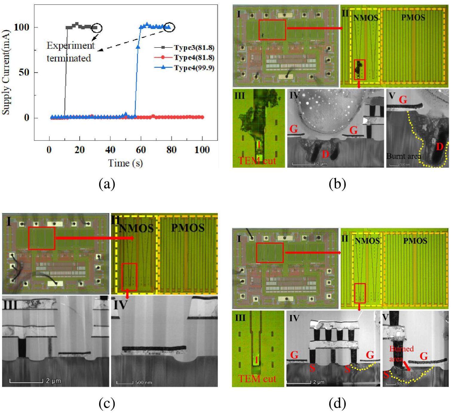
A high-magnification optical microscope (OM) and a transmission electron microscope (TEM) were used to further observe the SEE-sensitive regions of the chip and the burnout area. Some fault points were detected in the chips after the 81.8 MeV cm2 mg-1 and 99.9 MeV cm2 mg-1 SEE experiments for the types 3 and 4, respectively.
First, we examined the test chips using high-magnification OM. A noticeable burn mark was observed on the surface of the Type 3 chip after the 81.8 MeV cm2 mg-1 experiment (Fig. 5(b)). However, this chip had a multilevel design, and an upper layer of aluminum was added to its surface to ensure current flow. The internal structure of the NMOS was obscured by this top layer and could not be examined in detail by surface microscopy alone. Therefore, we performed TEM section sampling on the burned part of the aluminum wire based on the layout structure, using sections taken perpendicular to the drain. The TEM samples were prepared using the focused-ion-beam (FIB) cutting method, and the thin slices, which were only 1 μm thick, were observed via TEM. Accordingly, the complete morphologies of the source, drain, and gate of the NMOS were observed. The TEM findings revealed that the burned area in the Type 3 chip after exposure to 81.8 MeV cm2mg-1 corresponded to the drain metal wire and drain area. Hence, the drain of the NMOS with the SSD structure experienced the maximum current during SEE. In contrast, the surface of the Type 4 chip remained undamaged at the same LET of 81.8 MeV cm2mg-1 (Fig. 5(c)). However, an evident burn was detected on the surface of the Type 4 chip after exposure to 99.9 MeV cm2mg-1. TEM analysis revealed that this burn was near the source (Fig. 5(d)). The five images shown in Fig. 5 (b), (c), and (d) are enlarged step-by-step in the order of I, II, III, IV, and V (marked on the upper left corner of the pictures), and the next picture is a partially enlarged picture of the figure in the red box of the previous picture. This demonstrates that upon exposure to accelerating particles, the NMOS with the DSS structure generates the maximum current in the source.
The test results for the two devices were different. To analyze the causes and mechanisms underlying these differences, three-dimensional (3D) models of the two devices were established using Sentaurus TCAD to simulate the performance of the MOSFETs under SEE exposure [32-36] (Fig. 6). The device structure of the simulation model was determined by referring to the process structure of the driver and device layout shown in Fig. 2. In the vertical direction, the device consisted of a 10 μm epitaxial layer and a 2 μm buried layer connected to a 6 μm-deep PWELL. An asymmetric gate structure with a 0.2 μm-thick field oxide was used near the source under the gate oxide layer, while a thicker 0.55 μm oxide layer was used near the drain. In the horizontal direction, the gate width LG was 4 μm, and both the source (LS) and drain (LD) widths were 2 μm. The N+ drift region length LN+ was 2.4 μm. During the simulation, the drain voltage was biased at 20 V, while the gate and source voltages of the device were set to 0 V. These parameters were selected according to the commercial 0.35 μm BCD process used to fabricate the driver chips. The doping parameters of the devices were determined by the foundry, and the model parameters were calibrated according to the electrical parameters tested.
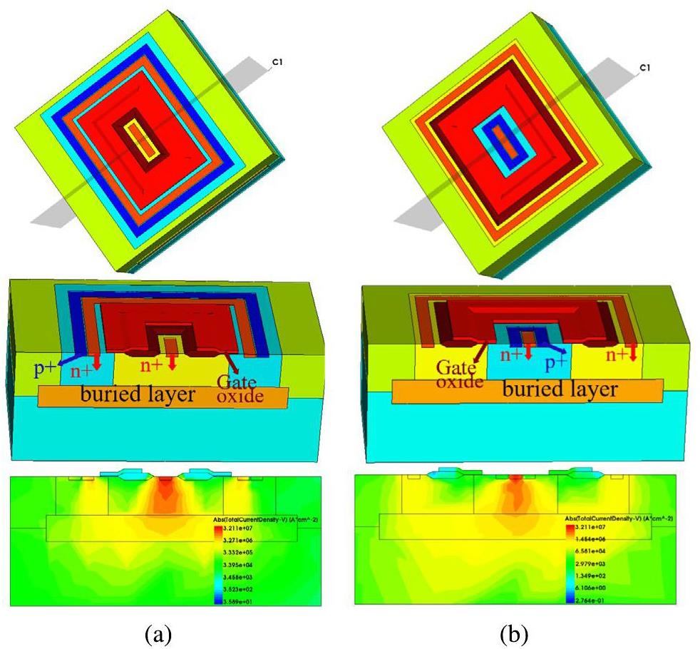
To analyze the SEE tolerance differences between the two structures, their current distributions under SEE effects were simulated using a heavy-ion irradiation model with a specific radius of 1 μm. The direction of the heavy-ion bombardment was perpendicular to the device. The concentration distribution of EHPs was generated using a Gaussian Model. The heavy-ion incidence time and LET value were 1 ns and 0.8 pC/μm, respectively. Under these conditions, the maximum drain current (IDMAX) and current distributions of the two device types were simulated under single-particle irradiation.
The first part of Fig. 6(a) or (b) shows the 3D models of the DSS or SSD MOSFETs, while the second and third parts depict the cross section of the first figure and internal current distribution of the two devices under SEE effects, respectively. The simulation results show that under single-particle irradiation, the IDMAX generated by the SSD and DSS structures were 1.16 mA and 0.73 mA, respectively.
In the SSD structure (Fig. 6(a)), the wider body area allowed more ion charges to be deposited during single-particle irradiation. Thus, more EHPs were generated under the same applied voltage, creating a base current and possibly turning on the parasitic BJT. This current generated a large current between the drain and source, eventually resulting in device burnout. In comparison, fewer EHPs were generated in the body region after single-particle irradiation in the DSS configuration (Fig. 6(b)). Thus, the current at the base of the parasitic BJT was smaller, which reduced the possibility of an unwanted parasitic BJT turning on. Therefore, the DSS structure is more resistant to single-particle irradiation than the SSD structure. However, in both SSD and DSS devices, the current was concentrated in the middle of the device (Fig. 6), which corresponded to the source and drain regions in the DSS and SSD structures, respectively. The burned areas observed after the SEE experiments (Fig. 5) were consistent with the simulation results (Fig. 6).
Conclusion
This article introduces a radiation-tolerant 20 V high-voltage driver prepared using the commercial 0.35 μm BCD process. In this driver, a comparator is used in the input unit, with the thick-gate-oxide NMOS of conventional high-voltage drivers replaced by a thick-gate-oxide PMOS and thin-gate-oxide NMOS. Accordingly, the hardened drivers exhibited an enhanced TID tolerance of 300 krad(Si). Additionally, a DSS structure was incorporated into all the NMOS devices to increase the overall SEE tolerance. The simulation and experimental results indicated that the DSS structure prevented unwanted parasitic BJT turn-on, enabling the designed chips to endure an LET of 81.8 MeV cm2mg-1. Moreover, the identification of the sensitive regions of devices with DSS and SSD structures based on morphological analysis after the SEE experiments indicates the feasibility of this strategy for effectively testing other radiation-tolerant designs. Because both the TID- and SEE-hardening methods proposed in this work utilize common commercial processes and do not require any changes in the process control conditions or process flows, they can be widely and economically applied to incorporate these novel integrated circuits in aerospace systems. Moreover, the reinforcement design and verification protocols proposed in this study can serve as a reference for similar optimization strategies and be combined with other radiation-hardening design methods, such as increasing the length of the N+ drift zone, to further enhance the radiation tolerance of the chips.
Space radiation effects in silicon devices
. IEEE T. Nucl. Sci. 12, 18-29 (1965). https://doi.org/10.1109/TNS.1965.4323897Evolution of total ionizing dose effects in MOS devices with Moore's law scaling
. IEEE T. Nucl. Sci. 65, 1465-1481 (2018). https://doi.org/10.1109/TNS.2017.2786140GERO: a general SCA-based readout ASIC for micro-pattern gas detectors with configurable storage depth and on-chip digitizer
. Nucl. Sci. Tech. 30, 131 (2019). https://doi.org/10.1007/s41365-019-0659-2Heavy-ion and pulsed-laser single event effects in 130-nm CMOS-based thin/thick gate oxide anti-fuse PROMs
. Nucl. Sci. Tech. 30, 80 (2019). https://doi.org/10.1007/s41365-019-0602-6SEU ground and flight data in Static Random Access Memories
. Nucl. Instrum. Methods Phys. Res., Sect. B. 245, 342-345 (2006). https://doi.org/10.1016/j.nimb.2005.11.125TID effect of MOSFETs in SOI BCD process and its hardening technique
. IEEE T. Nucl. Sci. 60, 1995-2001 (2023). https://doi.org/10.1109/TNS.2023.3281597ASET and TID characterization of a radiation hardened bandgap voltage reference in a 28-nm bulk CMOS technology
. IEEE T. Nucl. Sci. 69, 1141-1147 (2022). https://doi.org/10.1109/TNS.2022.3152496Comprehensive study on the total dose effects in a 180-nm CMOS technology
. IEEE T. Nucl. Sci. 58, 1347-1354 (2011). https://doi.org/10.1109/TNS.2011.2132145An analytical study of the effect of total ionizing dose on body current in 130-nm PDSOI I/O nMOSFETs
. IEEE T. Nucl. Sci. 66, 625-634 (2019). https://doi.org/10.1109/TNS.2019.2897278Total ionizing dose effect of gamma rays on H-gate PDSOI MOS devices at different dose rates
. Nucl. Sci. Tech. 28, 151 (2017). https://doi.org/10.1007/s41365-017-0295-7Monte Carlo reliability model for single-event transient on combinational circuits
. IEEE T. Nucl. Sci. 64, 2933-2937 (2017). https://doi.org/10.1109/TNS.2017.2772267SEU and SET of 65 Bulk CMOS Flip-flops and Their Implications for RHBD
. IEEE T. Nucl. Sci. 62, 2666-2672 (2015). https://doi.org/10.1109/TNS.2015.2490552Study of the correlation between the cutting edge current breakdown and the simulated lateral electrical field boundary in high resistivity silicon detectors with multi-guard ring structure
. IEEE T. Nucl. Sci. 47, 729-736(2000). https://doi.org/10.1109/23.856506A 15 V-Tolerant and Radiation-Hardened MOSFET Driver With Positive and Negative References
. IEEE Transactions on Aerospace and Electronic Systems 59, 851-857 (2022). https://doi.org/10.1109/TAES.2022.3191296Radiation-Hardened CMOS/SOS LSI Circuits
. IEEE T. Nucl. Sci. 23, 1613-1616 (1976). https://doi.org/10.1109/TNS.1976.4328550Development of a radiation-hardened lateral power MOSFET for POL applications
. IEEE T. Nucl. Sci. 56, 3456-3462 (2009). https://doi.org/10.1109/TNS.2009.2033922Design of 30 V high-voltage low-power radiation-tolerant analog switch IC
. IEEE T. Nucl. Sci. 69, 883-889 (2022). https://doi.org/10.1109/TNS.2022.3151409A radiation-hardened and ESD-optimized wireline driver with wide terminal common-mode voltage range
. IEEE T. Nucl. Sci. 65, 566-572 (2018). https://doi.org/10.1109/TNS.2017.2778942Total dose effects on the matching properties of deep submicron MOS transistors
. J. Semicond 35, 064007 (2014). https://doi.org/10.1088/1674-4926/35/6/064007A low-power, highly integrated radiation detection system for portable, long-duration monitoring
. IEEE Sens. J. 20, 10664-10678 (2020). https://doi.org/10.1109/JSEN.2020.2995288Analysis of angular dependence of single-event latchup sensitivity for heavy-ion irradiations of 0.18 μm CMOS technology
. IEEE T. Nucl. Sci. 62, 2539-2546 (2015). https://doi.org/10.1109/TNS.2015.2495101Dosimetry techniques and radiation test facilities for total ionizing dose testing
. IEEE T. Nucl. Sci. 65, 1440-1464 (2018). https://doi.org/10.1109/TNS.2018.2829864Design and offline testing of a resonant stripline beam position monitor for the IRFEL project at NSRL
. Nucl. Sci. Tech. 31, 70 (2020). https://doi.org/10.1007/s41365-020-00778-7An 8-Gs/s 12-Bit TIADC system with real-time broadband mismatch error correction
. IEEE T. Nucl. Sci. 65(12), 2892-2900 (2018). https://doi.org/10.1109/TNS.2018.2878875Temporal characteristic analysis of single event effects in pulse width modulator
. Nucl. Sci. Tech. 28, 29 (2017). https://doi.org/10.1007/s41365-017-0254-3Determining the effect of relative size of sensor on calibration accuracy of TEM cells
. Nucl. Sci. Tech. 30, 98 (2019). https://doi.org/10.1007/s41365-019-0618-yCompensation method for the coupling error between the EUT and TEM cell in E-field probe isotropic calibration
.Calibration of pulse transit time through a cable for EAS experiments
. Chinese Phys. C 38,Simulation study on performance optimization of a prototype scintillation detector for the GRANDProto35 experiment
. Nucl. Sci. Tech. 32, 51 (2021). https://doi.org/10.1007/s41365-021-00882-2Gamma measurement based on CMOS sensor and ARM microcontroller
. Nucl. Sci. Tech. 28, 122 (2017). https://doi.org/10.1007/s41365-017-0276-xSimulation study on cosmic ray background at large zenith angle based on GRAND Proto 35 coincidence array experiment
. Nucl. Sci. Tech. 32, 5 (2021). https://doi.org/10.1007/s41365-020-00841-3X-ray imaging and spectroscopy using low cost COTS CMOS sensors
. Nucl. Instrum. Methods Phys. B 248, 29-32 (2012). https://doi.org/10.1016/j.nimb.2011.09.007Simulation of gamma minitype reference radiation for calibration of personal dosimeter
. Nucl. Sci. Tech. 31, 12 (2020). https://doi.org/10.1007/s41365-019-0715-yShielding research of minitype reference radiation device based on Monte Carlo simulation
. High Power Laser Part. Beams 28, 168-175 (2016). https://doi.org/10.11884/HPLPB201628.160018Monte Carlo simulation investigation on the Minitype Reference Radiation employed for the calibration on gamma ray dose or dose rate meters
. J. Radiol. Prot 38, 407-421 (2018). https://doi.org/10.1088/1361-6498/aa9fb9The authors declare that they have no competing interests.

