Introduction
With advancements in space science and technology, an array of spacecraft has been deployed to fulfill various functions in space. However, the integrated circuits in these spacecraft are susceptible to cosmic rays, resulting in single-event effects (SEEs) and total ionizing dose effects (TIDs) [1]. Previous studies have indicated that the single-event upset (SEU) cross section of static random-access memory (SRAM) cells increases as the number of process nodes decreases [2, 3]. To mitigate the increasing severity of SEEs, researchers have proposed radiation-resistant reinforcement designs such as dual interlocked storage cell (DICE), which notably decrease the SEU cross section of the device [4-7]. Nonetheless, circuit-level reinforcement typically results in adverse ramifications, such as heightened power consumption, performance deterioration, and increased footprint [8, 9]. Silicon-on-insulator (SOI) technology has been introduced to minimize circuit area and power consumption while attenuating the sensitivity of integrated circuits to SEEs. This technology involves the introduction of a buried oxide (BOX) layer between the silicon film and substrate. This strategic placement mitigates the parasitic capacitance and short-channel effect of the device, thereby achieving comprehensive dielectric isolation of electronic components [10-13].
Although SOI technology can significantly reduce the cross section of transient irradiation effects, such as single-event transients (SETs), single-event latch-ups (SELs), and SEUs [14, 15], SOI devices exhibit decreased resistance to TIDs owing to the introduction of the BOX layer [16-19]. Cosmic rays can introduce trapped charges in the gate oxide, isolation oxide, and BOX layers, resulting in device parameter drift and degradation of electrical performance [20]. As technology nodes scale, the fully depleted silicon-on-insulator (FDSOI) process enhances the susceptibility to SEEs and the gate-control resistance by thinning the gate oxide and BOX layers [21]. However, the presence of a dopant trap region beneath the BOX layer constrains FDSOI back-gate bias and decreases circuit design flexibility. Furthermore, the shallow trench isolation and BOX layer of FDSOI are highly susceptible to TIDs, resulting in the formation of source–drain parasitic paths and a reduction in channel width [22, 23].
Previous studies have indicated that a novel configurable silicon on insulator (CSOI) structure can effectively mitigate the irradiation damage caused by TIDs and extend the back-gate bias range of the device [24, 25]. The CSOI process introduces two silicon layers: the top silicon film (SOI1) and underlying SOI2 layer located beneath the conventional BOX layer. In the CSOI device, back-gate biasing is achieved using independent electrodes. This approach not only hinders back-channel formation during irradiation, reduces the threshold voltage drift, and minimizes the leakage current [26, 27] but also efficiently regulates the electric field within the BOX layer. Through the reduction of the threshold voltage drift and leakage current, and by effectively regulating the internal electric field of the BOX layer, independent dynamic compensation of the TID [28] is achieved. CSOI implementation can regulate the drain region potential, thus suppressing SEEs.
The experimental validation and simulation analysis regarding the mitigation of TID through CSOI back-gate bias have been comprehensive. However, experiments and analyses on the dependence of CSOI-SRAM SEUs on the bias voltage when subjected to heavy-ion incidence at high linear energy transfer (LET) values are lacking. This study aimed to investigate the influence of the back-gate bias and supply voltage on the SEU of CSOI SRAM through a combination of experiments and technology computer aided design (TCAD) simulations. Additionally, in this paper, we propose a physical mechanism wherein the trend of variation in the SEU cross section with the supply voltage is opposite at high and low LET values. This exploration has significant implications for the understanding and reinforcement of CSOI SRAM against SEUs.
Sections 2 and 3 describe the experimental setup and discuss the experimental results, respectively. In Sect. 4, we describe the selection of the physical model for TCAD simulation and configuration of the simulation variables. We conducted qualitatively analysis to identify the sensitive state and sensitive region of the CSOI transistor, followed by simulations to explore the effects of back-gate bias and supply voltage on the SEU sensitivity of the CSOI SRAM. Through simulations that capture variations in physical quantities such as the transient pulse, potential, and collected charge of the SRAM off-state transistor under experimental parameters, we scrutinize and derive the physical mechanism underlying the influence of back-gate bias and supply voltage on the SEU cross section. This analysis explains and validates the experimental findings. Finally, Section 5 presents the concluding remarks.
Experimental Setup
Experimental device description
The CSOI devices utilized in the experiments were fabricated using the 0.18 μm FDSOI process, and the primary parameters and transistor sizes are listed in Table 1. The overall structure comprised two silicon layers (SOI1 and SOI2) and two oxygen-embedded layers (BOX1 and BOX2). Electronic components were fabricated on the top silicon film, whereas the intermediate silicon layer, SOI2, was positioned between the two oxygen-embedded layers to serve as a back-gate electrode. This electrode enabled adjustment of the electrical performance and resistance of the device to SEUs by modifying the voltage applied to SOI2. Consequently, both the electrical characteristics of the device and SEU resistance could be tailored by varying the voltage of SOI2. The presence of the BOX layer mitigated the parasitic bipolar amplification effect and decreased leakage currents.
| Parameters | Value (nm) |
|---|---|
| Thickness of the top silicon film (TSOI1) | 65 |
| Thickness of oxygen embedded Layer 1 (TBOX1) | 145 |
| SOI2 layer thickness (TSOI2) | 150 |
| Thickness of oxygen-embedded layer 2 (TBOX2) | 145 |
| INV_P channel length | 320 |
| INV_N channel length | 200 |
| Transfer_N channel length | 200 |
A 4k-bit 6T-SRAM provided by the Institute of Microelectronics of the Chinese Academy of Sciences (IMCAS) was employed to explore the SEU resistance of SRAM fabricated using the CSOI process under varying back-gate biases. The chip package, which houses a 64 × 64-bit memory array with dimensions of approximately 1.45 mm × 1.45 mm, features a bit cell footprint of 10μm × 8 μm. Within the memory cell, N-type transistors share an NSOI electrode, denoted by Vnsoi, whereas P-type transistors share a PSOI electrode, denoted by Vpsoi. The back-gate biasing of the SRAM ranges from -10 to 10 V. The circuits were encapsulated in DIP-28 packages. Considering the utilization of high-LET heavy ions in the experiment, the devices were decapped to ensure adequate penetration of the heavy ions.
Experimental setup for heavy-ion irradiation
For the experiments, Ta ions were selected from the TR5 terminal at the Heavy Ion Research Facility in Lanzhou (HIRFL) and the High Energy Heavy Ion Radiation Terminal (HERT) at the Space Environment Simulation and Research Infrastructure (SESRI) at Harbin Institute of Technology. The ion parameters are listed in Table 2, with the fluence set to 5×10⁶ ions/cm2 for each experimental group. To achieve a uniform heavy-ion beam within the irradiated area, we adjusted the scanning current and frequency, coupled with precise control of the irradiated area by manipulating the slit size. Ta-ion irradiation was conducted in air, which was facilitated by the ability of the heavy-ion beam to reach the sensitive region of the device even after passing through a Ti window and traveling several microns in the atmosphere. The heavy ions traversed through a vacuum/air transition foil before impinging on the device. To detect the injection, we positioned an injection detector along the ray trajectory before the device under test. The LET of the ions from the device surface to the detector was adjusted by either inserting an energy attenuator (aluminum foil) into the trajectory of heavy-ion incidence or employing angled ion impingement.
| Heavy-ion parameters | TR5 Terminal | HERT |
|---|---|---|
| Ion type | Ta | Ta |
| Range (μm) | 60 | 51 |
| LET (MeV·cm2/mg) | 86.1 | 87.3 |
| Fluence (ions/cm2) | 5×10⁶ | 5×10⁶ |
| Energy (MeV) | 942 | 759 |
Experiments were conducted to investigate the impact of NSOI and PSOI electrodes, as well as the power supply voltage, on the SRAM SEUs. Before irradiation, 55+AA-type data were pre-written into the SRAM memory cells with a dynamic reading of the SRAM memory content during irradiation. Any discrepancies between the read and write results were recorded by the test system as either a 0-1 or 1-0 upset, depending on the type of upset observed. These experiments were performed at room temperature while maintaining a flux of approximately 15000 ions/cm2·s to negate flux effects. A nominal supply voltage of 1.8 V was applied to the test system to simulate the normal operating state of the device. Back-gate biases were uniformly set to zero to assess the effect of the supply voltage on SRAM SEU. Six supply voltage biases were selected: pull down 20% (1.44 V), pull down 10% (1.62 V), pull down 5% (1.71 V), nominal voltage (1.80 V), pull up 10% (1.98 V), and pull up 20% (2.16 V). These biases were selected to examine the effect of the supply voltage on SEU.
The SEU overturning cross section is calculated as
Discussion of Experimental Results
The analysis revealed that the total number of SEEs observed in this experiment solely comprised single-bit upsets, with no occurrences of errors, such as multiple-bit upsets or single-event functional interrupts. Figure 1(a) depicts the dependence of the SEU cross section on Vnsoi at LET =86.1 MeV·cm2/mg, where Vpsoi was set to zero for all experiments. Notably, the SEU cross section experienced decreases of 47.31%, 87.82%, and 93.23% at Vnsoi =-2, -6, and -10 V, respectively, compared with the scenario with zero back-gate bias. Conversely, Figure 1(b) shows the dependency of the SEU cross section on Vpsoi under the same LET conditions, with Vnsoi set to zero across all experiments. Here, the SEU cross section had decreases of 40.50%, 78.79%, and 83.77% at Vpsoi =2, 6, and 10 V, respectively, compared with the scenario with zero back-gate bias.

Table 3 presents the impact of various back-gate bias combinations on the SEU cross section for LET = 87.3 MeV·cm2/mg. It demonstrates that the application of negative Vnsoi and positive Vpsoi can effectively mitigate the SEU cross section. Notably, when the sum of the absolute values of the back-gate bias applied to the N-type and P-type transistors of the SRAM was equal, a larger ratio of |Vnsoi|/|Vpsoi| resulted in lower sensitivity of the SRAM to SEU. Moreover, under identical magnitudes of back-gate bias, the negative bias applied to the NSOI electrode of the N-type transistor exhibited superior effectiveness against SEU compared with the positive bias applied to the PSOI electrode of the P-type transistor.
| Vpsoi (v) | Vnsoi (v) | Number of SEUs | SEU cross section (cm2/bit) |
|---|---|---|---|
| 2 | 0 | 51 | 1.5×10⁻¹⁰ |
| 1 | -1 | 47 | 1.4×10⁻¹⁰ |
| 0 | -2 | 43 | 1.3×10⁻¹⁰ |
| 3 | -1 | 24 | 7.2×10⁻¹¹ |
| 2 | -2 | 19 | 5.7×10⁻¹¹ |
| 1 | -3 | 19 | 5.7×10⁻¹¹ |
| 3 | -3 | 2 | 6.0×10⁻¹² |
Figure 2(a) shows the relationship between the SEU cross section and supply voltage at LET = 86.1 MeV·cm2/mg. Notably, at the nominal applied circuit voltage of 1.8 V, 61 single-bit upsets were recorded, whereas only one single-bit upset occurred at VDD =1.62 V, and 158 single-bit upsets were observed at VDD =1.98 V. Furthermore, a 10% increase in the supply voltage resulted in a significant increase in the SEU cross section of 161.67%. This observation suggested that the variation in the thickness of the drain depletion region with changes in VDD contributed to the escalation of the SEU cross section. Further analysis of this mechanism is provided in detail in Section 4.

Figure 2(b) depicts the relationship between the SEU cross section and supply voltage at LET = 87.3 MeV·cm2/mg. Compared with the SEU cross section of 3.3E-10 cm2/bit at nominal voltage, the SEU cross section decreased by 95.40% and 96.30% for a pull-down VDD of 10% and 20%, respectively, and increased by 125.93% and 165.74% for pull-up VDD of 10% and 20%, respectively.
When VDD was below 1.62 V, the resultant drain voltage did not enable the CSOI to establish an effective drain depletion region capable of efficiently collecting the charge excited by heavy ions. Consequently, the SEU cross section exhibited minimal variation with the supply voltage and remained significantly lower than the SEU cross section observed at the nominal voltage.
For VDD exceeding 1.71 V, the SEU cross section experienced a rapid escalation with increasing supply voltage, reaching a plateau after a pull-up of 10%. We posit that the supply voltage range from a 5% pull-down to a 10% pull-up constituted the interval in which the width of the space-charge region underwent a significant variation in response to voltage changes. Within this range, any alteration in the supply voltage significantly affected the capability of the device to collect unbalanced carriers. However, when VDD surpassed 1.98 V, the width of the space-charge region ceased to vary significantly. This stabilization was attributed to the power function relationship governing the width of the space-charge region with a reverse bias voltage.
SEU Simulation and Discussion
TCAD Physical Model Setting
To achieve a comprehensive understanding of the mechanisms driving the observed experimental phenomena, we employed TCAD semiconductor device-simulation software to develop a CSOI model. After parameter calibration, we utilized SDEVICE to construct a 6T-SRAM for the CSOI process. This section presents an investigation of the relationship between the SEE and parameters such as the heavy-ion incidence position, back-gate voltage, and supply voltage to elucidate the phenomena detailed in Section 3.
Figure 3 depicts the CSOI device model developed for this simulation. The SRAM core memory cell comprised two pairs of input and output cross-coupled inverters (N1, P1; N2, P2). In the stable storage state of the cell, the word line was maintained at a low level, causing the transmission transistors N3 and N4 to be in the off state. Consequently, the n0 node stored datum “1”, whereas the n1 node stored data “0”.

Heavy-ion incidence was modeled by incorporating lateral diffusion via a Gaussian distribution with a trajectory radius of 0.015 μm. Given the significant generation of carriers due to SEEs, mechanisms including Fermi–Dirac statistics [30] as well as Shockley—Read–Hall (SRH) and Auger recombinations [31] (indirect and Russo–Cherese composites) were incorporated into the simulation.
Susceptibility of SEUs to the incidence position of heavy-ion
The simulation results indicated that the off-state transistor exhibited the highest sensitivity to SEUs, as shown in Fig. 4. In this state, electrons generated by heavy ions within the off-state NMOS channel swiftly migrated towards the drain owing to the carrier-collecting effect and bipolar amplification effect facilitated by the drain PN junctions. Consequently, the peak SET current reached its maximum magnitude. Conversely, in the transmission state, the source and drain terminals were biased, rendering them unable to establish a potential difference in the carrier drift. Consequently, only a minimal number of carriers migrated to the source and drain terminals concurrently owing to the diffusion motion, resulting in a significantly reduced SET current compared with the off state. In the open state, the electric potential difference between the source and drain was zero, impeding the drain from efficiently collecting the electron-hole pairs generated by the channel. Hence, the on-state NMOS transistor exhibited the lowest sensitivity to SEUs.
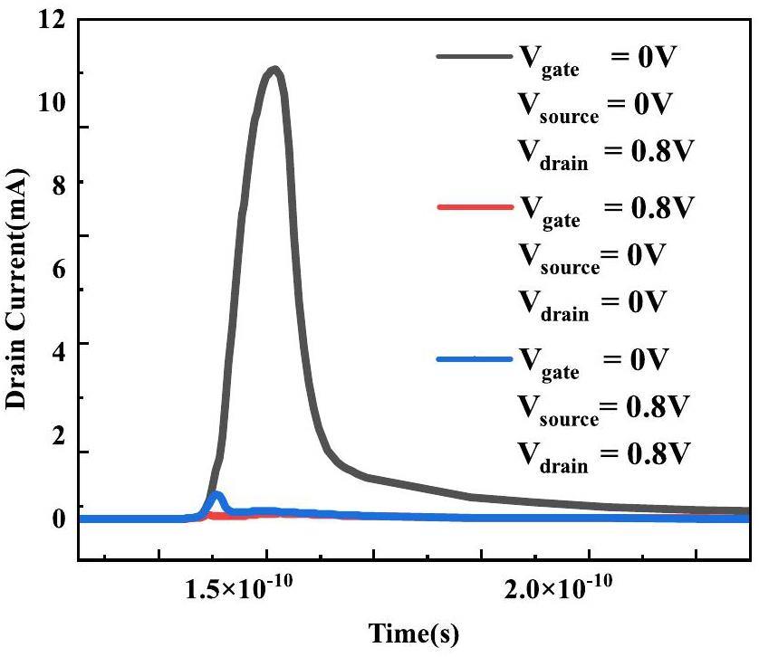
Figure 5(a) depicts the charge collected at the drain end of the device when heavy ions impinged vertically on the off-state NMOS and PMOS of the SRAM at various positions. The findings indicated that the sensitive region of the SRAM was at the drain–gate PN (D-G) junction of the off-state transistor. Given the similarity in the physical mechanism of triggering SEEs for both off-state transistors, this study exclusively analyzed the NMOS transistor.
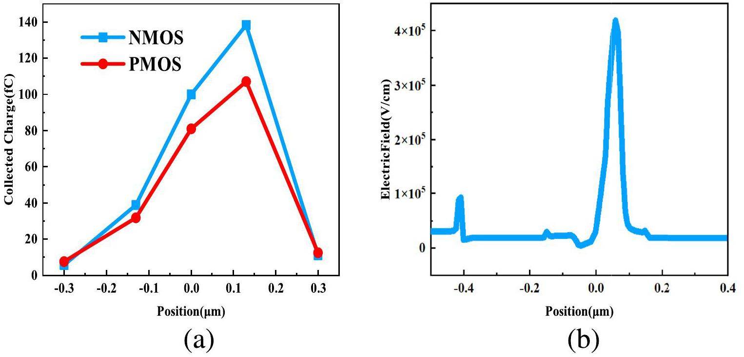
As depicted in Fig. 5(b), compared with other regions within the body area, the depletion region of the D-G junction in the off-state MOS exhibited the highest electric field strength. Consequently, the device achieved the highest efficiency in collecting carriers generated by heavy ions incident on the D-G junction. Consequently, the resulting current pulse from the heavy ions impacting this region demonstrated the shortest peaking time and accumulated the most charge. Conversely, when the incident position lay within the source region, the carrier drift motion was required to overcome the potential barriers of both the source–gate (S-G) and D-G junctions for collection by the drain electrode. Consequently, the source electrode exhibited the lowest sensitivity to SEEs, with only a fraction of carriers generated by heavy-ion ionization undergoing drift motion. Instead, the majority contributed to a diffusion current driven by concentration gradients, characterized by an SET pulse current featuring a small peak but a significant tail current.
Conversely, owing to their higher electron mobility compared with that of holes, electrons are more readily collected by the drain, resulting in the generation of a pulse current. Consequently, the SEE sensitivity of NMOS, in which electrons constitute the majority carriers in the source–drain, surpasses that of PMOS. This discrepancy is evident in Fig. 5(a), where the peak charge collected by NMOS exceeded that collected by the PMOS.
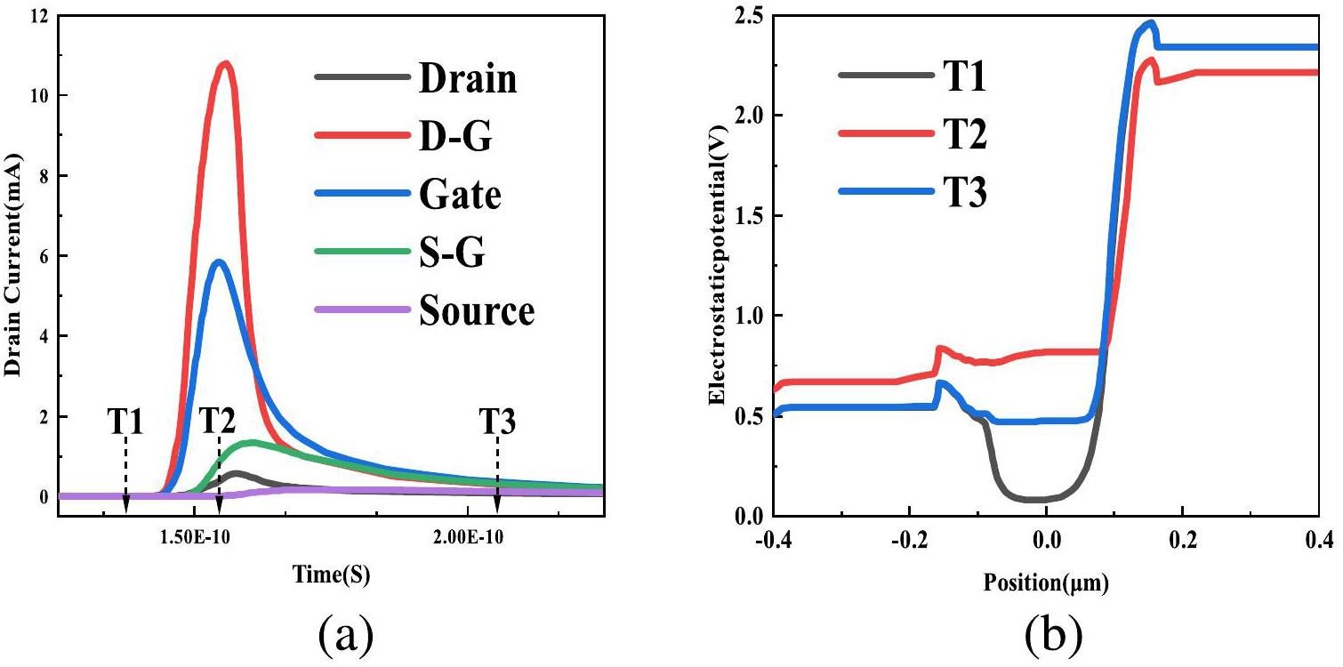
Furthermore, as depicted in Fig. 6(a), to elucidate the mechanism of heavy-ion impact on transistor-level devices and subsequently analyze the effect of back-gate voltage on the SEU cross section, we simulated the electrostatic potential of the devices at three distinct moments: before (T1), during (T2), and after (T3) heavy-ion incidence. Figure 6(b) shows that heavy ions with sufficient LET striking the sensitive region of an NMOS transistor generated a significant number of carriers within the device. Electrons were predominantly collected by the drain, thereby reducing the drain potential, whereas the accumulation of holes after electron excitation increased the body potential. This reduction in the potential barrier between the body and source–drain induced a zero or even positive bias in the base–emitter junction of the parasitic bipolar transistor, thereby instigating a bipolar amplification effect that augmented the pulse current.
Relationship between SEU occurrence and back-gate bias
Figure 7(a) and (b) illustrate the variations in the cross-sectional potential distributions with the back-gate bias for NMOS and PMOS transistors after heavy-ion incidence, respectively. As |Vnsoi| and |Vpsoi| increased, the drain barrier height increased, making it more challenging for electrons to traverse the D-G barrier and reach the drain. Consequently, fewer carriers were collected at the drain of the off-state MOS, thereby attenuating the parasitic bipolar amplification effect and decreasing the SEE sensitivity of the device. This augmented the self-recovery capability of the SRAM and elevated the LET threshold.
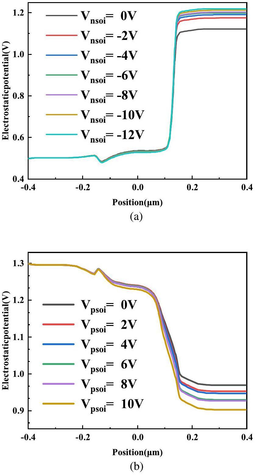
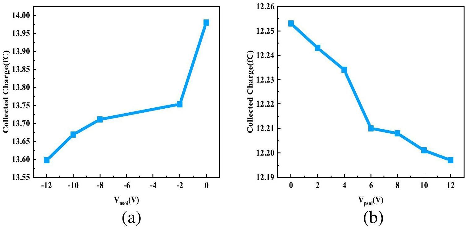
Figure 8 shows the relationship between the collected charge and back-gate bias. As |Vsoi| increased from 0 to 10 V, the NMOS collected charge decreased by 2.22%, and the number of SEUs in the experiment decreased by 94.24%. The PMOS collected charge decreased by 0.43%, and the number of SEU in the experiment decreased by 83.78%. This observation supported the experimental finding that the inhibition of SEUs was more pronounced with Vnsoi than with Vpsoi.
In addition, when analyzing the experimental data, we observed that the device exhibited the most significant charge reduction when the absolute value of |Vsoi| increased from 0 to 2 V. The slopes of the curves in Fig. 1(a) and (b) are 5.24×10⁻¹¹ cm2/bi·V and 4.48×10⁻¹¹ cm2/bi·V, respectively, which were the highest among all the ranges. This suggests that this voltage level offered the highest rejection efficiency for SEU occurrences. Considering both the circuit power and SEU cross section, the back-gate bias combination of Vnsoi=-2 V and Vpsoi=2 V was considered more suitable.
Impact of Supply Voltage on SEUs
Because the semiconductor power consumption is directly proportional to the square of the supply voltage, a viable strategy for minimizing power usage involves lowering the supply voltage. However, note that the susceptibility of the SRAM to SEUs is influenced by the supply voltage. Consequently, a comprehensive examination of the SEU sensitivity of CSOI SRAM across various supply voltage levels must be conducted. The SRAM soft error rate is described by the following model [34]:
According to the formula
In contrast, the collected charge (QColl) is a strong function of the particle LET value and supply voltage, which characterizes the number of carriers collected at the drain during heavy-ion incidence [39]. For MOSFET devices, the depletion-region thickness can be calculated using the following equation:
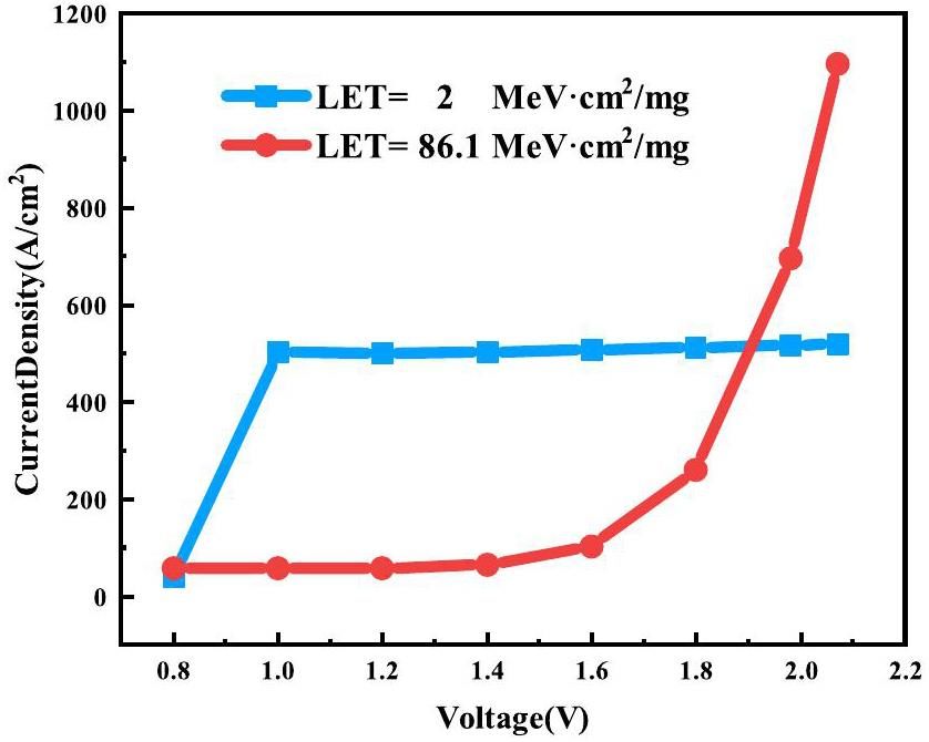
In the low core voltage state, the limited number of holes generated in the body region by low-LET heavy ions fails to effectively diminish the source–body potential barrier. Consequently, these holes are unable to traverse the depletion region between the source and body and are released through the ground. The accumulation of holes in the body region elevates the electric potential, prompting a significant flow of electrons to be collected by the drain through the depletion region between the drain and body. Conversely, heavy ions with high LET values generate a significant number of carriers, which significantly reduces the potential barriers between the source and body. Thus, most of the holes generated in the body region by these heavy ions cross the depletion region between the source and body and are released to the ground. This lowers the electric potential of the body region, suppresses the bipolar amplification effect, and results in partial electron collection by the drain. Therefore, in the low-voltage state, the current density produced by heavy ions with high LET values is lower than that produced by heavy ions with low LET values.
In the high-core-voltage state, the drain depletion region extends sufficiently to collect almost all the electrons generated by the low-LET heavy ions, causing the current density from these ions to saturate after the core voltage increases to 1.0 V. As the core voltage increases, the width of the drain-body depletion region expands, enhancing the electron collection efficiency of the drain. Simultaneously, the elevated drain voltage increased the electric potential of the body region, thereby strengthening the bipolar amplification effect. Consequently, the current density from heavy ions with high LET values increases rapidly with core voltage. In the high-voltage state, the current density from high-LET heavy ions surpasses that from low-LET heavy ions.
The physical process of widening the drain-junction depletion region owing to an increase in the supply voltage, as discussed in [40], results in the enlargement of the SEU cross section. This phenomenon is referred to as mechanism II in this paper.
Figure 10 shows that for low-LET heavy-ion incidence, Qcrit and QColl increased with the supply voltage. However, the number of carriers generated by heavy ions of a specific LET value remained constant and was unaffected by variations in VDD. The depletion region expanded sufficiently to capture the excited carriers when the supply voltage exceeded 1 V. Therefore, when the increase in VDD allowed the drain–depletion region to gather the majority of carriers, the magnitude of the change in Qcrit and QColl with respect to VDD resulted in a notable disparity. This was evidenced by the increase in Qcrit surpassing the increase in QColl. During this phase, mechanism I prevailed, resulting in a decrease in the SEU cross section with an increase in the supply voltage.
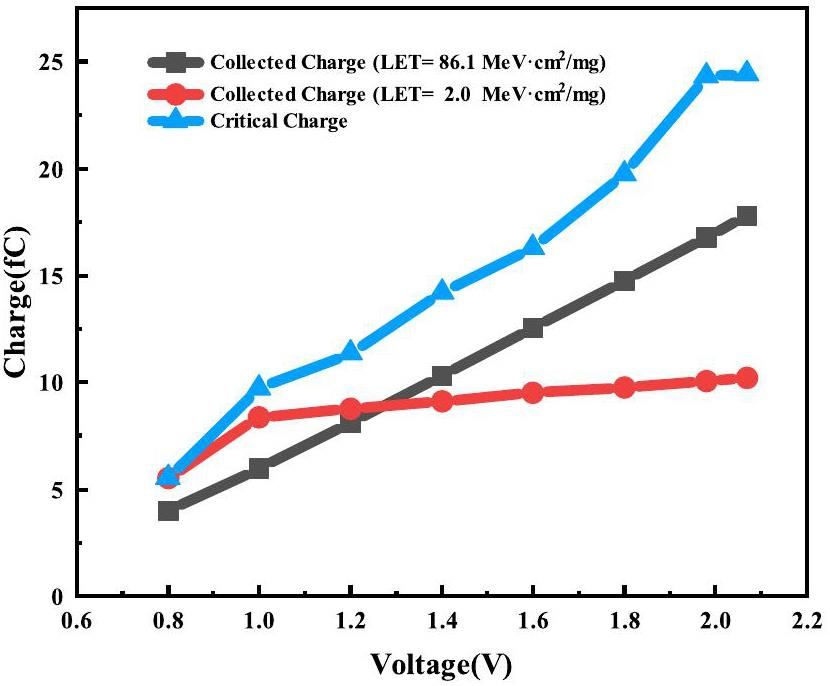
However, for high-LET heavy-ion incidence, as shown in Fig. 10, because of its capacity to deposit a greater amount of energy in the sensitive region of the device, the excitation carriers were not entirely collected by the depletion layer at a voltage of VDD of 1.98 V. The collected charge increased rapidly with increasing VDD. At this juncture, Mechanism II was dominant.
During the competition between the two mechanisms mentioned above, the notable increase in the SEU cross section of CSOI SRAM under Ta-ion irradiation with increasing supply voltage can be attributed to the increase in the depletion layer thickness and the parasitic bipolar current induced by the increasing VDD. Although mechanism II prevailed in this 0.18 μm node test and simulation, the conflicting influences of mechanisms I and II in small-node technology and low-core voltage scenarios merit further comprehensive investigation.
Conclusion
The experimental results demonstrated that both negative N-type and positive P-type transistor back-gate biases can effectively enhance the SEU resistance of an SRAM memory cell. Moreover, we observed that the impact of Vnsoi is superior to that of Vpsoi when subjected to the same bias voltage magnitude. Maintaining the absolute value of |Vsoi| between 2 V and 6 V not only ensures low power consumption of the circuit but also aids in suppressing SEU occurrences. Through TCAD simulations, this study investigates the sensitive location of the CSOI SRAM and explored the influence of back-gate bias and supply voltage on the SEE sensitivity of the SRAM. For a specific range and LET value of heavy-ion incidence, we observed that the drain-body potential difference of the NMOS device increased with back-gate bias. This increase results in an increase in the barrier height between the body and source–drain, consequently suppressing the parasitic bipolar amplification effect and reducing the SEU cross section of the CSOI SRAM.
In the context of SRAM, we observed that two competing mechanisms exist for SEU occurrence. First, an increase in the supply voltage results in an escalation of the critical charge and a reduction in the circuit-sensitive volume. Second, an increase in the supply voltage widens the depletion region, resulting in an augmentation in the device’s collected charge and sensitive volume. In most cases, these two mechanisms coexist and compete, potentially resulting in varying competitive outcomes. Specific process nodes and LET values have crucial roles in determining the nature of the competition. Thoroughly evaluating the SEU cross section at various LET values and core voltages and conducting bias experiments to determine the worst-case scenario for SRAM performance during ground testing are crucial. Neglecting to consider these factors may result in an underestimation of the circuit SEU cross section.
Total-ionizing-dose radiation effects in AlGaN/GaN HEMTs and MOS-HEMTs
. IEEE Trans. Nucl. Sci. 60, 4074-4079 (2013). https://doi.org/10.1109/TNS.2013.2278314Technology dependence of stuck bits and single-event upsets in 110-, 72-, and 63-nm SDRAMs
. IEEE Trans. Nucl. Sci. 70, 1861-1869 (2023). https://doi.org/10.1109/TNS.2023.3295435Evaluation of the single-event-upset vulnerability for low-energy protons at the 7- and 5-nm bulk FinFET nodes
. IEEE Trans. Nucl. Sci. 70, 1687-1693 (2023). https://doi.org/10.1109/TNS.2023.3246085SEU tolerance of FinFET 6T SRAM, 8T SRAM and DICE memory cells
, in Paper presented at the 7th Annual Computing and Communication Workshop and Conference (CCWC) (The orientational dependence of single event upsets and multiple-cell upsets in 65 nm dual DICE SRAM
. Microelectron. Reliab. 94, 24-31 (2019). https://doi.org/10.1016/j.microrel.2019.01.013Verification of SEU resistance in 65nm high-performance SRAM with dual DICE interleaving and EDAC mitigation strategies
. Nucl. Sci. Tech. 32, 139 (2021). https://doi.org/10.1007/s41365-021-00979-8Power optimized SRAM cell with high radiation hardened for aerospace applications
. Microelectron. J. 103,9-T SRAM cell for reliable ultralow-power applications and solving multibit Soft-Error issue
. IEEE Trans. Device Mater. Reliab. 16, 172-182 (2016). https://doi.org/10.1109/TDMR.2016.2544780Novel quadruple-node-upset-tolerant latch designs with optimized overhead for reliable computing in harsh radiation environments
. IEEE Trans. Emerging Top. Comput. 10, 404-413 (2022). https://doi.org/10.1109/TETC.2020.3025584Reduction of the reverse short channel effect in thick SOI MOSFET’s
. IEEE Electron Device Lett. 18, 90-92 (1997). https://doi.org/10.1109/55.556090Total dose induced latch in short channel NMOS/SOI transistors
. IEEE Trans. Nucl. Sci. 45, 2458-2466 (1998). https://doi.org/10.1109/23.736486A high speed and low power on CMOS/SOI technology
. IEEE Trans. Electron Devices. 40, 2103-2104 (1993). https://doi.org/10.1109/16.239769Compact model for tunnel diode body contact SOI n-MOSFETs
. IEEE Trans. Electron Devices. 66, 249-254 (2019). https://doi.org/10.1109/TED.2018.2873590Single event transient and TID study in 28 nm UTBB FDSOI technology
. IEEE Trans. Nucl. Sci. 64, 113-118 (2017). https://doi.org/10.1109/TNS.2016.2627015SEU performance of schmitt-trigger-based flip-flops at the 22-nm FD SOI technology node
. Microelectron. Reliab. 146,Impact of back-gate bias and device geometry on the total ionizing dose response of 1-transistor floating body rams
. IEEE Trans. Nucl. Sci. 59, 2966-2973 (2012). https://doi.org/10.1109/TNS.2012.2223828The effects of total ionizing dose on the SEU cross-section of SOI SRAMs
. Electronics. 11, 3188 (2022). https://doi.org/10.3390/electronics11193188Comparison of total ionizing dose effects in 22-nm and 28-nm FD SOI technologies
. Electronics. 11, 1757 (2022). https://doi.org/10.3390/electronics11111757Comparison of total ionizing dose effects in SOI FinFETs between room and high temperature
. IEEE Trans. Nucl. Sci. 69, 359-366 (2022). https://doi.org/10.1109/TNS.2021.3129784TID degradation mechanisms in 16-nm bulk FinFETs irradiated to ultrahigh doses
. IEEE Trans. Nucl. Sci. 68, 1571-1578 (2021). https://doi.org/10.1109/TNS.2021.3076977Evaluation of SEU performance of 28-nm FDSOI flip-flop designs
. IEEE Trans. Nucl. Sci. 64, 367-373 (2017). https://doi.org/10.1109/TNS.2016.2630022Simulation of total ionizing dose effects technique for CMOS inverter circuit
. Micromachines. 14, 1438 (2023). https://doi.org/10.3390/mi14071438Simulation of total ionizing dose (TID) effects mitigation technique for 22 nm fully-depleted silicon-on-insulator (FDSOI) transistor
. IEEE Access. 8,Dependence of temperature and back-gate bias on single-event upset induced by heavy ion in 0.2 μm DSOI CMOS technology
. IEEE Trans. Nucl. Sci. 68, 1660-1667 (2021). https://doi.org/10.1109/TNS.2021.3094669Total ionizing dose radiation effects hardening using back-gate bias in double-SOI structure
. IEEE Trans. Nucl. Sci. 69, 453-461 (2022). https://doi.org/10.1109/TNS.2022.3145027An effective method to compensate total ionizing dose-induced degradation on double-SOI structure
. IEEE Trans. Nucl. Sci. 65, 1532-1539 (2018). https://doi.org/10.1109/TNS.2018.2824402The total ionizing dose response of a DSOI 4Kb SRAM
. Microelectron. Reliab. 76, 714-718 (2017). https://doi.org/10.1016/j.microrel.2017.07.068DSOI FET - A novel TID tolerant SOI transistor
, in Paper presented at the 12th IEEE International Conference on Solid-State and Integrated Circuit Technology (ICSICT) (Characteristic charge collection mechanism observed in FinFET SRAM cells
. IEEE Trans. Nucl. Sci. 69, 1833-1839 (2022). https://doi.org/10.1109/TNS.2022.3188993Numerical modelling of degenerate and nondegenerate semiconductors with the Fermi-Dirac distribution
, in Paper presented at the 2016 International Conference on Electrical and Information Technologies (ICEIT) (Effect of field dependent mobility and simultaneous consideration of both SRH and auger recombination on the analytical modeling of internal quantum efficiency of a si-solar cell
, in Paper presented at the TENCON 2011 - 2011 IEEE Region 10 Conference (Automatic TCAD model parameter calibration using autoencoder
, in Paper presented at the 2023 International Conference on Simulation of Semiconductor Processes and Devices (SISPAD) (Analytical models of effective DOS, saturation velocity and high-field mobility for SiGe HBTs numerical simulation
, in Paper presented at the 2010 International Conference on Simulation of Semiconductor Processes and Devices (Reliability for nanomagnetic logic (NML) readout circuit under single event effect
. Microelectron. J. 46, 20-26 (2015). https://doi.org/10.1016/j.mejo.2014.09.014Prediction of single event upset critical charge and sensitive volume depth by energy deposition analysis of low energy protons
. Radiat. Eff. Defects Solids. 175, 1093-1108 (2020). https://doi.org/10.1080/10420150.2020.1806838The increased single-event upset sensitivity of 65-nm DICE SRAM induced by total ionizing dose
. IEEE Trans. Nucl. Sci. 65, 1920-1927 (2018). https://doi.org/10.1109/TNS.2018.2816583Collected charge analysis for a new transient model by TCAD simulation in 90 nm technology
. IEEE Trans. Nucl. Sci. 57, 1869-1875 (2010). https://doi.org/10.1109/TNS.2010.2053944Impact of technology and voltage scaling on the soft error susceptibility in nanoscale CMOS
, in Paper presented at the 2008 IEEE International Symposium on Defect and Fault Tolerance of VLSI Systems (Single-event-transient effects in silicon-on-insulator ferroelectric double-gate vertical tunneling field effect transistors
. Sci. China Inf. Sci. 63,Depletion region thicknesses in diffused junctions
. IEEE Trans. Electron Devices. 20, 659-660 (1973). https://doi.org/10.1109/T-ED.1973.17721The authors declare that they have no competing interests.

