Introduction
The interface between Si and transition metals is of paramount importance in various engineering applications, including microelectronic systems [1] and nanotechnology [2]. The electrical, thermal, and mechanical responses of the Si/transition metal interface are crucial factors in determining the overall performance of the engineered system [3, 4]. In recent years, the field of nuclear energy has witnessed a surge in interest in betavoltaic cells [5-7]. Betavoltaic cells offer a number of advantages, including a long operational life, stable output, ease of integration, high energy density, and high environmental adaptability. As a result, betavoltaic cells are an ideal alternative in various scenarios where the use of fossil fuel or chemical batteries is not feasible, such as in remote sensing applications in extreme environmental conditions, medical implantable devices, and microelectromechanical systems (MEMS) [8]. Tritium betavoltaics hold more promise than others owing to the highly specific activity of solid tritium compounds, low shielding requirements, and relatively high availability of tritium as a byproduct of CANDU® nuclear reactors [9]. A number of studies have been conducted on the incorporation of tritides into monocrystalline Si transducers [10-12]. Tritiated titanium is renowned for its low decay ray energy, excellent chemical stability, and high safety. Titanium is capable of adsorbing and storing tritium in the solid state at a pressure of approximately 1.33d-5 Pa, forming tritiated titanium. This phenomenon results in a high storage density and rapid absorption rate of tritium. The equilibrium dissociation pressure is approximately 10-5 Pa at room temperature [13]. Samples containing Si/transition metal interfaces are prepared via various vapor-phase film growth techniques. The deposition of transition metals on monocrystalline Si substrates is known to result in the formation of polycrystalline films. In fact, for tritium betavoltaic cells with three-dimensional (3D) micro- and nanostructured semiconductors, existing studies have loaded tritium directly onto the semiconductor in the form of a gas. To obtain a higher amount of the radioisotope tritium, this approach requires exploring the possibility of obtaining tritium-absorbing metal thin films with the largest possible surface area and uniformly distributed in the 3D micro- and nanostructures to act as tritium carriers. Ti thin films, which act as the tritium absorbing material in betavoltaic cells, have a direct influence on the amount of tritium adsorbed and its diffusion path, thereby affecting the energy conversion efficiency and output power density of the cell. Thus, the performance of tritium cells can be significantly improved by optimizing the Ti film preparation process.
Magnetron sputtering is a widely utilized technique for the deposition of Ti films. The preparation process has a substantial influence on the surface morphology, grain size, and texture of the obtained Ti films, thereby significantly impacting their functional properties [14-16]. The sputtering power is an important factor that influences the microstructure of Ti films as it controls the rate of atomic deposition. Chen et al. [17] demonstrated that the deposition rate has a significant effect on the microstructure of Ti films deposited on the Si(100) surface via magnetron sputtering. As the deposition rate increased, a transition was found to occur from a random growth orientation to the (002) preferred growth orientation. Researchers have imaged the nanoamorphous structure of Ti films, which is characterized by the presence of nanocrystals within an amorphous matrix. Chawla et al. [18] reported that the grain size of Ti films increased with increasing sputtering power and substrate temperature. At 100 and 150 W, the (101) and (002) preferred growth orientations were observed for deposition on glass substrates. In a related study, Han et al. [19] investigated the impact of sputtering powers ranging from 80 to 120 W on the properties of the obtained Ti thin films deposited in deep holes. They reported that as the sputtering power increased, the thin films exhibited a tendency to form columnar structures. Moskovkin et al. [20] reported that at the lowest power density, the c axis of α-Ti[001] was perpendicular to the substrate, and the (002) planes were parallel to the substrate. As the discharge power density increased during deposition, additional Ti(100) planes parallel to the substrate appeared. Finally, at the highest power density, (100) planes parallel to the substrate were mainly observed during deposition. These structural changes caused corresponding changes in the hardness of the film. However, the reason behind the observed peak in the (100) planes remains unclear. These studies formulated a hypothesis regarding the nucleation and growth mechanism of Ti films on Si(100) substrates, but further research is still needed to study this deposition process.
Atomic-scale simulations, including density functional theory (DFT), molecular dynamics (MD), and Monte Carlo (MC) simulations, have proven to be valuable tools for investigating the atomic-scale behavior of metal/ceramic interfaces, as well as for studying interfacial energetics [21-23], heat transport properties at interfaces [24], and dynamic processes at surfaces and interfaces [25, 26]. First-principles methods are highly accurate for the determination of energy changes and for acquiring electronic information in the context of small system models. The team led by Añez employed first-principles calculations to investigate the Ti atom adsorption process on the Si(111) and Si(100) surfaces [21-23]. The interatomic interactions at the Ti–Si interface were analyzed from a thermodynamic perspective. The results indicated that the mixing of the Ti–Si interface is enhanced by the presence of defect regions on the substrate surface, which emphasizes the importance of Si diffusion in determining the structure of the Ti–Si mixed layer.
Over the past decade, MD simulations for plasma surface interactions have emerged as a crucial tool for investigating a range of plasma phenomena, including sputtering, etching, injection, and deposition [27-30]. These simulations can replicate the nucleation and growth behaviors of thin films. While periodic boundaries are commonly employed in MD simulations, ensuring that the model is sufficiently large to maintain the authenticity of the simulation is highly important. Moreover, variations in the element type and structure of the target within the simulation system can result in differences in the interatomic potential functions [31]. Conventional MD simulations are typically limited to temporal scales of hundreds of nanoseconds due to the constraints imposed by the size of the simulated system and the interatomic potential functions. Consequently, this limits the range of possible outcomes that can be observed in the simulation system, making it challenging to capture slow but critical structural evolution processes. MC simulations determine atomic displacement probabilities on the basis of thermodynamic barriers, enabling the sampling of a broader phase space and often permitting surface structures to attain thermal equilibrium on shorter time scales [32-34]. Among the aforementioned algorithms, the primary advantage of the time-stamped force-bias Monte Carlo (tfMC) method is its capacity to preserve the temporal scale. Although the tfMC method does not explicitly incorporate time, it establishes a correlation between the simulation and the time scale by incorporating deterministic forces acting on the atoms into a stochastic algorithm for atomic displacement. This results in a markedly increased acceptance rate of atomic displacement, thus accelerating the attainment of equilibrium in the simulated system. Namakian and colleagues employed a sequential MD/tfMC algorithm to simulate the deposition behavior of Cu on a TiN substrate [26]. The transformation of the Cu film on the TiN(001) substrate from a body-centered cubic (BCC) structure to a face-centered cubic (FCC) structure, accompanied by the formation of nanotwins, was observed and experimentally verified. Furthermore, they identified distinct film growth mechanisms on the TiN(111) surface at the Ti-terminated end and the N-terminated end. Gao et al. [25] reported significant variations in the microstructure of Cu films deposited on different substrate surfaces. These variations were more pronounced on the Si(100) planes and in the vertical arrangement of higher-position atoms on the (110) crystal planes. Notably, specific deposition characteristics were observed on the (111) crystal planes. Compared with the C(111) surface, the top atoms exhibited a more pronounced annular distribution and a relatively smooth surface. Considerable research has been conducted on the topic of MD simulations of Cu deposition on Si substrates [35, 36]. However, studies on MD simulations of Ti films are scarce.
This study aims to investigate the nucleation and growth mechanisms of Ti films on Si(100) substrates via computational simulations. The primary objective of this study is to analyze the impact of different deposition energies on the microstructure of the obtained Ti films as well as the process of Ti nucleation and growth on Si(100) substrates. Section 2 provides a comprehensive account of the computational methodology employed in this study and the model configuration. The principal simulation outcomes are presented and discussed in Sect. 3, while the conclusions are drawn in Sect. 4.
Computational details
DFT
All DFT calculations were performed using the DS-PAW software [37]. The Perdew–Burke–Ernzerhof (PBE) generalized gradient approximation (GGA) was employed to model the exchange correlation between electrons. A plane-wave cutoff energy of 400 eV was utilized in all calculations, with a 15-Å-thick vacuum layer set in the Z-direction of the geometry. The Methfessel–Paxton integration scheme was employed for sampling the Brillouin zone at the Monkhorst–Pack special points [38]. The following calculation was performed with an energy convergence criterion of 10-6 eV and a force convergence criterion of 0.01 eV ⋅Å-1. The atomic adsorption energy was determined through the following equation:
To gain further insights into the adsorption and diffusion behavior of Ti on the Si(100) surface, the transition state search (TSS) method was employed to calculate the optimal diffusion paths and the corresponding energy barriers between different adsorption sites. Additionally, the k-point mesh utilized for climbing-image nudged elastic band (CI-NEB) calculations was set to 6 × 6 × 1, while the energy convergence criterion was set at a constant value. Conversely, the force convergence criterion was modified to 0.01 eV⋅Å-1.
Model of Ti atom deposition and simulation methodology
All the MD simulations were conducted via the large-scale atomic/molecular massively parallel simulator (LAMMPS) [39]. A Si(100) surface structure was constructed as the substrate via the LAMMPS, with the x-, y-, and z-axes oriented along the [011], [
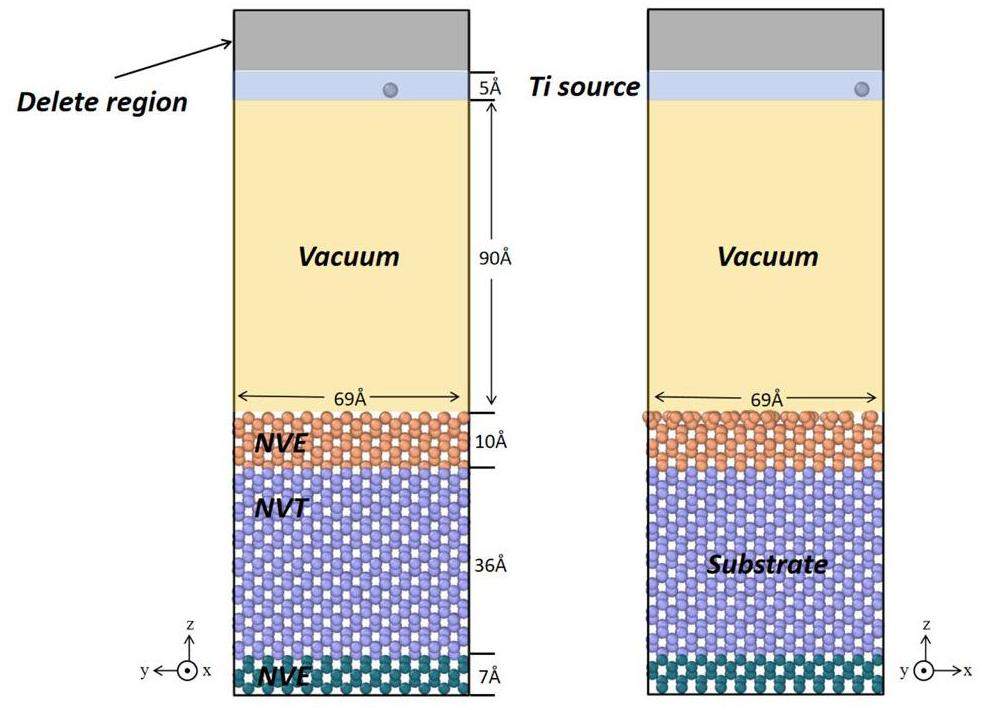
Relevant studies have demonstrated that the relaxation process in vapor deposition simulations significantly impacts the final microstructure of the thin film. To more accurately simulate the growth behavior of the Ti atoms on the Si(100) surface during deposition, a scheme combining the tfMC method and MD simulations was employed in this work. The tfMC approach does not consider the atomic velocity; therefore, the concept of temperature lacks physical significance; the only relevant ‘temperature’ is the sampling temperature of the system. The key parameter for determining the success of tfMC simulations is the maximum displacement length Δ of the lightest element in the system. A larger Δ results in a longer effective simulation time. However, Δ must also be selected to be sufficiently small to meet the equilibrium requirements. In this work, the properties of metallic Ti and semiconducting Si with perfect lattices were tested separately. The results indicate that setting ΔTi to 0.1 and ΔSi to 0.1 ensures a broader sampling phase space while minimizing precision loss.
Simulation of Ti atom deposition
The deposition process is divided into two stages: The first involves the mutual diffusion of the Ti and Si atoms, whereas the second involves the self-diffusion of the deposited Ti atoms. To accurately depict the Ti deposition behavior and investigate the film growth mechanism, the Tersoff potential function developed by Plummer et al. [40] was utilized to describe the interaction between Ti and Si, and the EAM potential function developed by Mendelev et al. [41] was utilized to characterize the interactions between the Ti atoms. Prior to the commencement of the simulation, a hybrid scheme incorporating both potential functions was validated. To facilitate the study, it was assumed that the incident particle approaches the surface following a direction perpendicular to it. Depending on the specific deposition parameters, a Ti atom is randomly emitted to the substrate within the incident layer. The velocity of the incident atom is determined by the given incident energy Ein, which can be calculated as follows:
| Energy (eV) | Rate ( |
|---|---|
| 0.1 | 6.3 |
| 0.5 | 14.2 |
| 1 | 20.1 |
| 5 | 44.9 |
| 10 | 89.8 |
The substrate temperature was set to 500 K during the thin-film deposition process. The temperature of 500 K was selected based on the fact that it provides the optimal kinetic energy for promoting film growth during Ti deposition. The diffusion of Ti atoms is significantly more pronounced at this temperature than at other temperatures, which affects the orientation, nucleation, and growth process of the film, ultimately resulting in a higher-quality film. Furthermore, a series of control experiments were conducted at 300 K and 0.1 eV to investigate the phase transition phenomenon during the growth of the Ti films. The system achieved thermal equilibrium by undergoing a 20-ps relaxation period under the NVE ensemble before the deposition process was initiated. For the Nose-Hoover thermostat and the Nose-Hoover barostat, the time constants for temperature and pressure relaxation toward the desired values were set to 100 and 1000 times the time step, respectively. A specified number of Ti atoms were randomly inserted in the deposition area, with each newly deposited atom required to be at least one cutoff radius (6.9 Å) away from the previously deposited atom. Following the completion of the deposition process, an NVT ensemble relaxation was employed to control the temperature fluctuations resulting from the kinetic energy transfer during successive collision events of the deposited Ti atoms. To ensure the full execution of both types of diffusion processes in the deposition simulation, 50 deposition cycles were carried out, with 300 atoms deposited per cycle. Therefore, each cycle comprised the following steps: MD deposition, MD thermal balance, tfMC relaxation, and MD thermal balance. All the simulation results were visualized using the OVITO software. The surface atomic structure was analyzed via the polyhedral template matching (PTM) method, with the root-mean-square deviation (RSMD) cutoff set to 0.1.
Results and discussion
Ti diffusion behavior on the Si(100) surface
The cubic Si bulk was initially optimized, and the energy and force were made to converge using a Monkhorst–Pack mesh of 4 × 4 × 4 k-points. The optimized lattice constant was found to be 5.47 Å, which is in agreement with the results reported by Añez et al. [23] and experimental data (5.43 Å) [42], with a discrepancy of no more than 1%. The structure-optimized Si(100) surface, which contains four Si dimer structures, is depicted in Fig. 2. The Si atoms in the dimers are shown in distinct colors for ease of differentiation. The structure was obtained through cell expansion and modification of the cut surface on the basis of the Si(100)p(2×2) surface. The Si(100) surface model used in this work contains eight layers of atoms. The formation energy of the dimers on this surface is 1.68 eV, and these dimer structures are highly similar. Furthermore, the x-, y-, and z-directions of the model correspond to the [010], [001], and [100] directions of the Si crystal, respectively. The dangling bonds on the bottom surface are saturated by H atoms. The bottom four layers of atoms are fixed in the subsequent calculations to simplify the model. Such a research approach has been demonstrated to be feasible on numerous occasions. Additionally, the k-point mesh utilized for the calculations was set to 6 × 6 × 1.
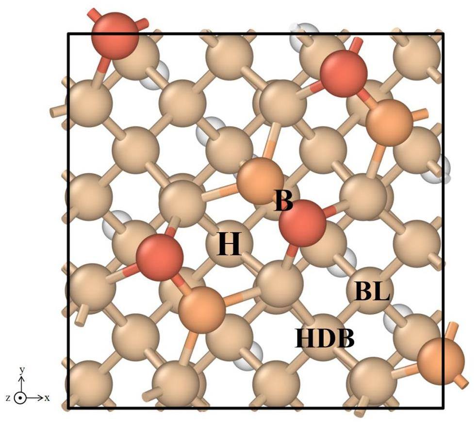
The dimer structure of the Si(100) surface results in the existence of four distinct adsorption sites for individual Ti atoms on the periodic substrate, which are labeled with letters in Fig. 2. The adsorption energies of individual Ti atoms for different sites on the Si(100) surface are presented in Table 2. Among the four sites, site B is energetically less stable, and its structure optimization results are similar to those of site H, which will not be considered in the rest of this study.
| Atom/Position | Adsorption energy |
|---|---|
| H | -5.65 |
| HDB | -4.36 |
| BL | -4.96 |
| B |
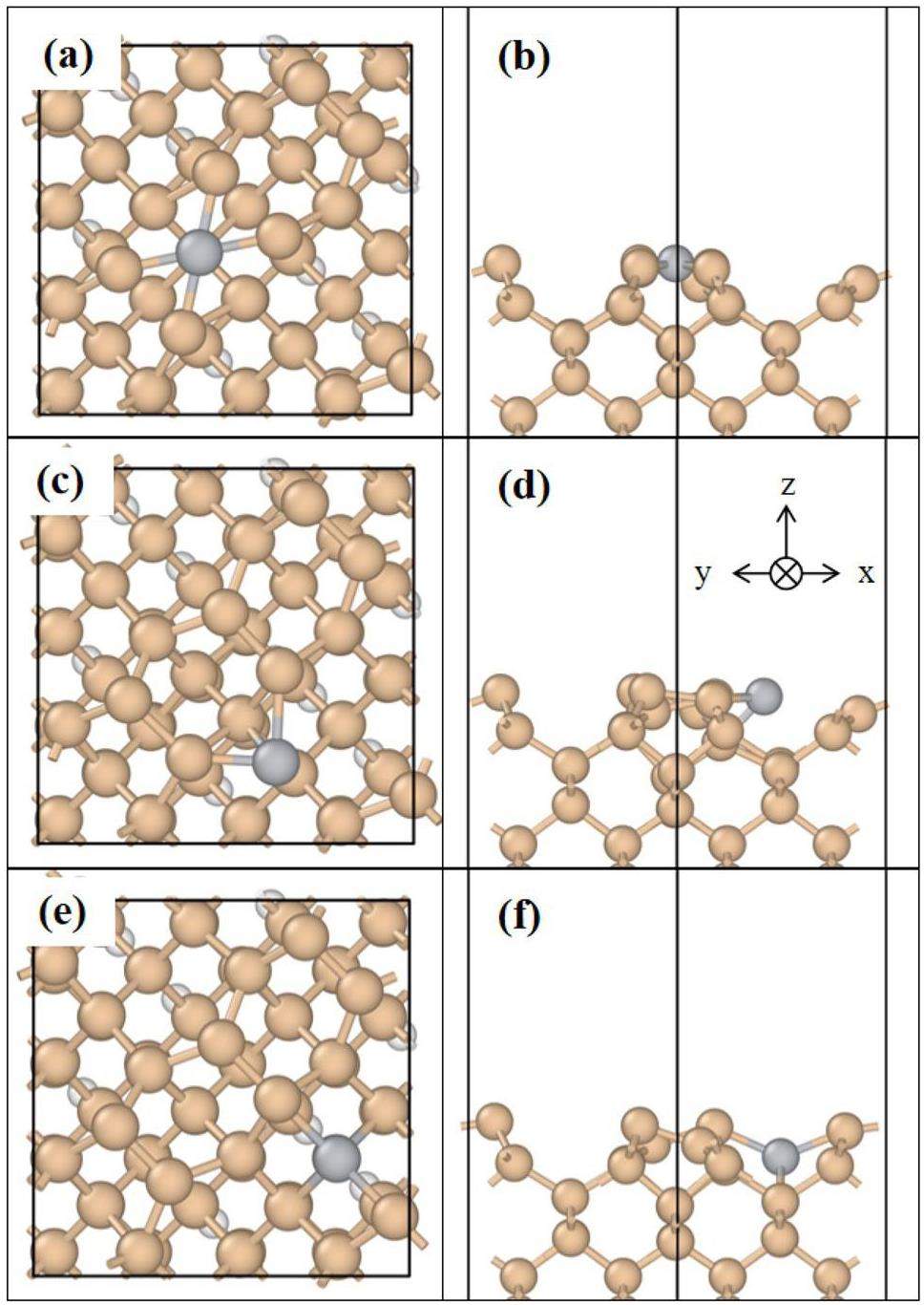
The results indicate that the Ti atoms are more favorably adsorbed at the H-site, with an adsorption energy of -5.65 eV. The Ti atoms at the H-site are bonded with the Si atoms in the four surrounding dimers. There are two types of Ti–Si bonds, with bond lengths of 2.40 and 2.42 Å, as shown in Fig. 3(a, b). The bond length between the Si atoms in the dimer is observed to increase as a consequence of the interaction between the Ti and Si atoms. Concurrently, the asymmetry of the Si atoms in the two dimers bonded to them is reduced because of the adsorption of the Ti atoms at the HDB-sites. Nevertheless, the atomic environments of the two are not equivalent, and the lengths of the Ti‒Si bonds are still different, namely 2.67 and 2.53 Å. This is not consistent with the results reported by Añez et al. This discrepancy can be attributed to the fact that the surface model in this work has a larger periodic unit than that used by Añez et al. The structures of the Ti atoms adsorbed at the H- and HDB-sites exhibit a relatively low degree of symmetry, which is influenced by the presence of neighboring dimers. Consequently, the calculations presented in this work are in better agreement with the adsorption properties of individual Ti atoms on the Si(100) surface. When a Ti atom is adsorbed at the BL-site, the Si atoms bonded to the Ti atom exhibit three distinct atomic environments. The Ti atom interacts with the Si atoms on the two subsurfaces of the nondimer (Fig. 3(e, f)) with a bond length of 2.60 Å. Furthermore, this Ti atom is bonded to the Si atoms of the two neighboring dimers. In fact, the two Si atoms have different atomic environments. In contrast to the surface model presented in Ref. [23], the adsorption sites are positioned as far as possible inside the model rather than on the periodic boundaries. This approach ensures the acquisition of more realistic data on the adsorption energy. Changes in the bond length between Ti and Si affect the electron density distribution and local geometry, which in turn change the capacity of the adsorption sites to provide electrons. In the case of short Ti–Si bond lengths, the increased electron density in the vicinity of the Ti atoms facilitates electron transfer from the adsorption sites, thus decreasing the adsorption energy. Conversely, as the Ti–Si bond length increases, the electron density decreases, and the adsorption energy increases.
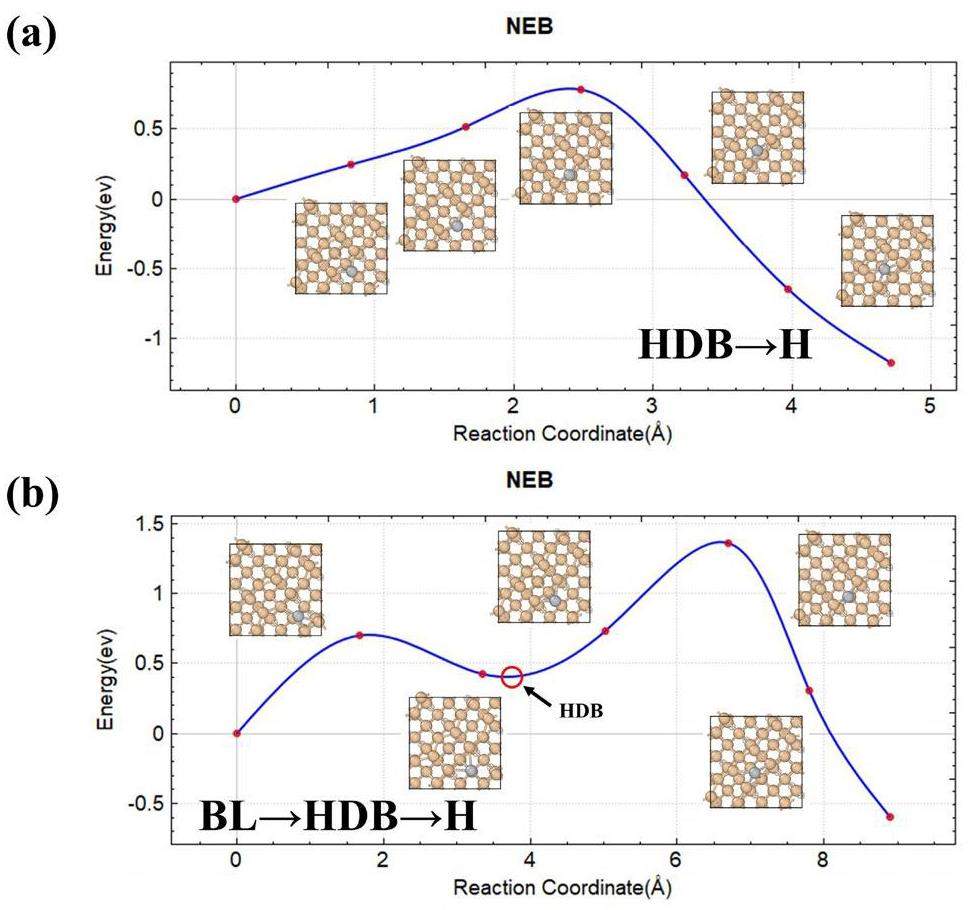
The precise calculation of the adsorption energy of individual Ti atoms enabled the determination of the minimum energy paths for the diffusion of the Ti atoms from the first nearest-neighbor HDB- and BL-sites to the H-site. Five points were set between the initial and final positions via linear interpolation. The results of the TSS are presented in Fig. 4. The diffusion of the Ti atoms from the HDB-site to the H-site necessitates the crossing of the Si atoms in the two dimers to which they are bonded. As previously discussed, the two Si atoms regain some symmetry due to the presence of the Ti atom at the HDB-site. Consequently, at this specific stage, the Ti atoms diffuse following a roughly linear trajectory toward the H-site. The system energy reaches its maximum when the Ti atom is directly above the two Si atoms. Notably, the calculated shortest diffusion path from the BL-site to the H-site reveals that the Ti atoms must traverse two potential barriers throughout the entire process. The Ti atoms initially reach the first nearest-neighbor HDB-site and subsequently diffuse to the most stable H-site. These results indicate that the adsorption of Ti atoms at the H-site on the Si(100) surface is highly stable and that the diffusion of Ti atoms requires overcoming a high potential barrier.
MD/MC simulations of Ti atom deposition
In accordance with the deposition scheme outlined in Section 2, 15,000 atoms were deposited on the Si(100) surface in approximately 25 layers. The range of incident atomic energies was considered to be from 0.1 to 5 eV. Fig. 5 shows the initial island growth and island aggregation behavior of the Ti films at incident energies of 0.1 and 5 eV. To quantify the changes in the deposition structure over time, the number of simulated cycles was used as a proxy for the simulation time in the analysis. At the beginning of the deposition simulation, the Ti atoms readily form 3D islands locally (Fig. 5(a, d)) because of the adsorption of the Ti atoms on the Si(100) surface. At a low incident energy, the islands gradually coalesce, resulting in two-dimensional (2D) growth in the xy-plane with minimal change in the island height. As the islands continue to grow in a 2D manner, the film thickness increases. The islands merge and gradually cover the entire substrate, as illustrated in Fig. 5(b, c). In the case of a high incident energy, the distribution of the Ti atoms is slightly deeper, as illustrated in Fig. 5(e). In other words, the surface is covered with the Ti atoms at an earlier stage, leading to the subsequent film growth occurring more rapidly. In the subsequent stage, the stacking of the Ti atoms is the primary growth mode, resulting in a notable increase in the rate of film growth [43]. In addition, the layer coverage of the Ti and Si atoms near the Ti–Si interface (located at Z = 60) was quantified (Fig. 6). To eliminate the possibility of obtaining random results, the coverage results were compared in the range between 20% and 80%. The results show that the diffusion of the Si and Ti atoms is not significant at a low incident energy. Elevated incident energies enhance Ti ion implantation efficiency. As a d-block transition metal, the lower mixing ratio of Ti to Si is analogous to that of Co to Si in a previous work [44]. Despite the lower mixing ratio at the interface, a small number of Si atoms still exert a moderate influence on the growth of the Ti films. The detachment of Si results in the formation of irregular defects at the interface, which may act as sites for the preferential nucleation of the Ti atoms. Following the initial nucleation, the deposition of the Ti atoms continues around these defect sites, resulting in a film growth pattern that exhibits specific orientations or the formation of early grain boundaries and stress concentration regions.
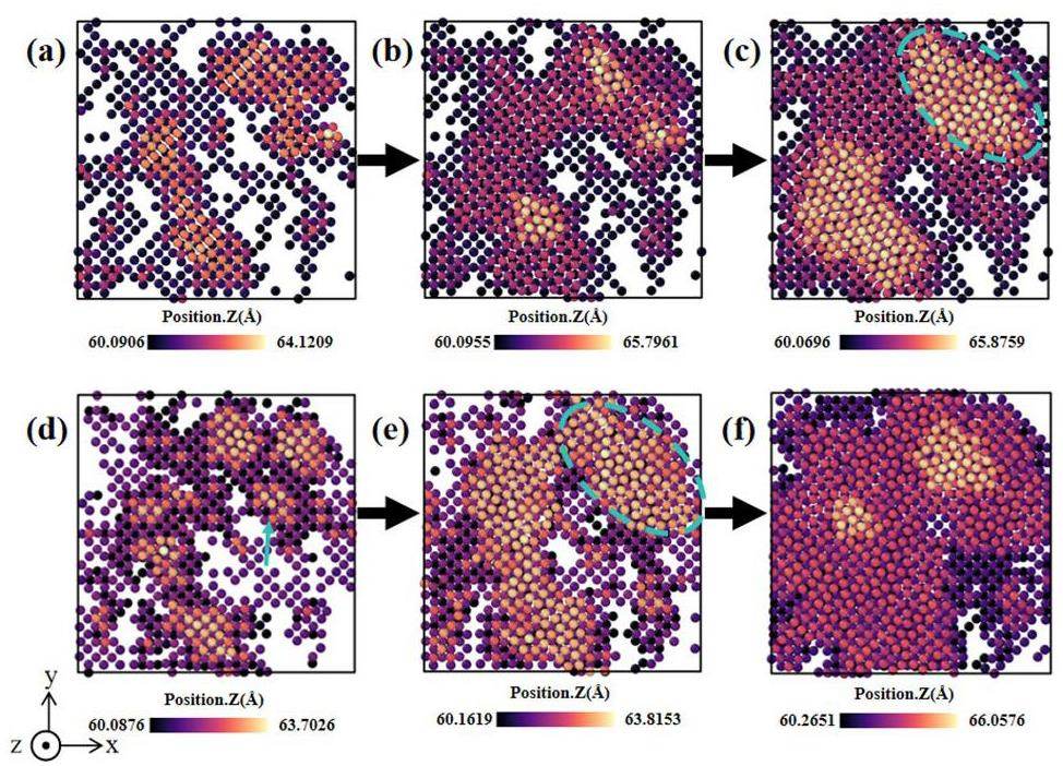
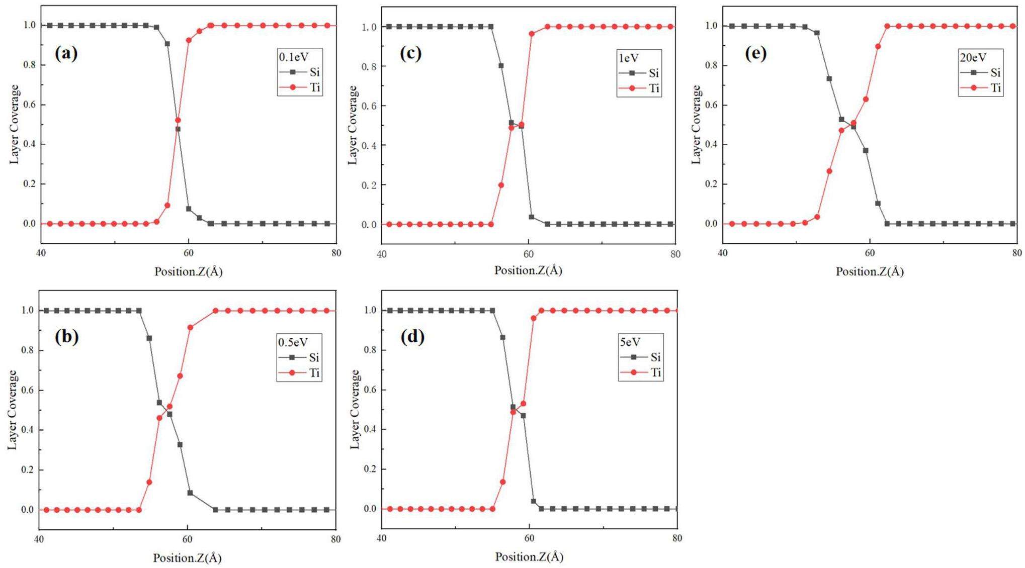
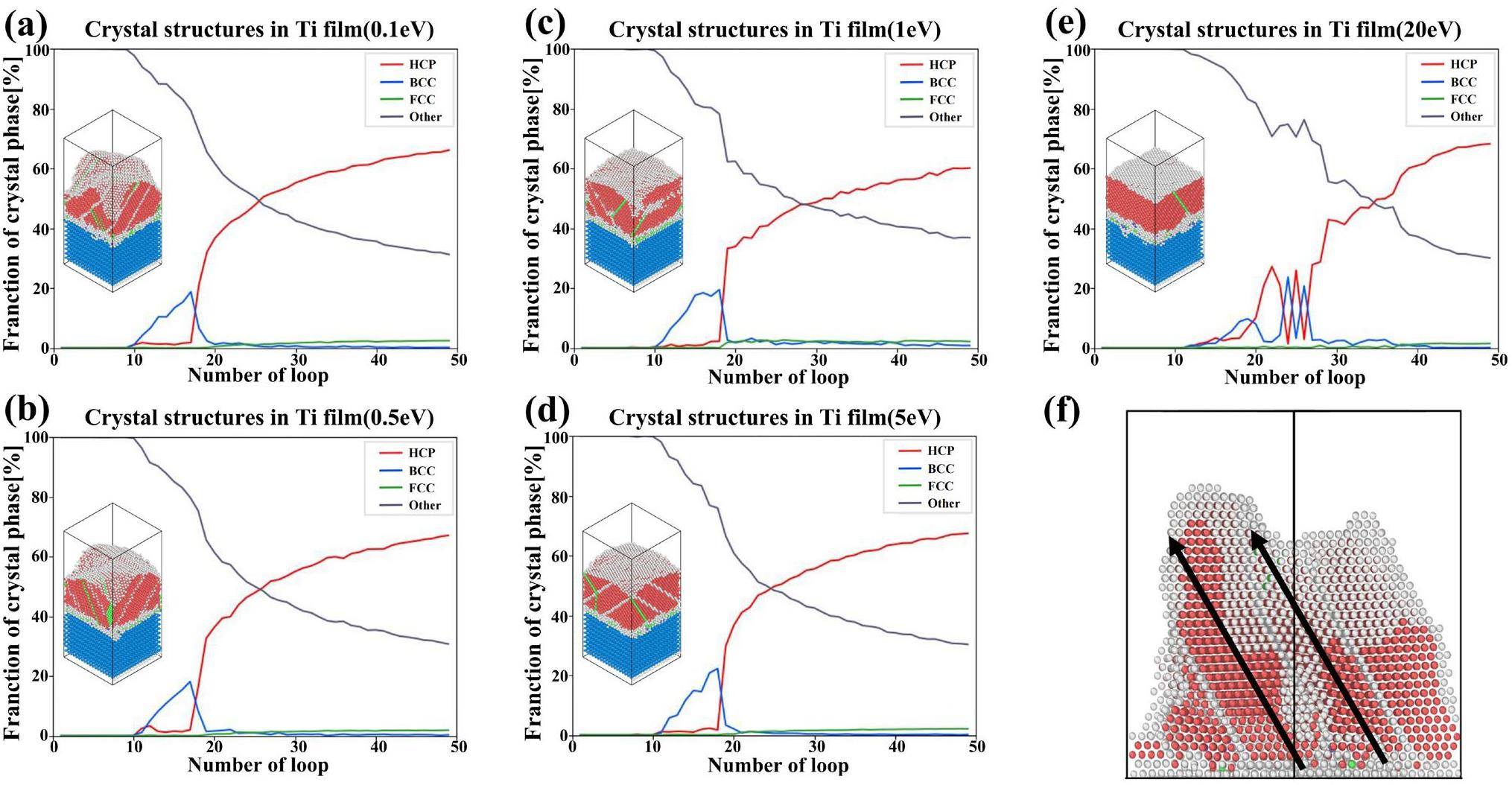
Figure 7 shows the evolution of the crystal structure of the Ti films as a function of the simulation time at different incident energies. The results show that the Ti films deposited on the Si(100) surface at 500 K eventually exhibit the hexagonal close packed (HCP) structure, which accounts for up to 60% of the crystal structure. At a high sputtering power, the Ti atoms migrate on the substrate surface and occupy the available equilibrium positions on the pre-existing Ti film lattice, resulting in the formation of a columnar structure in the film [45]. The film grows at an angle relative to the substrate plane, which is consistent with findings from previous studies [46]. During the initial stages of film deposition, the Ti films predominantly exhibit the BCC phase. After 10 cycles, the substrate surface becomes covered by the Ti atoms, indicating that the growth of the Ti thin film has entered the Ti stacking phase. At this stage, the formed Ti film is influenced by the surface structure of the Si(100) substrate. The atomic arrangement is looser, and the space utilization is lower than the previous stage. At this stage, the Ti films locally exhibit the BCC structure on the surface. The regions with this structure act as buffer regions between the subsequently formed regions with the HCP structure and the Si substrate until the number of Ti atoms reaches a certain level, at which point the BCC structures disappear. Notably, the stable growth phase of the HCP structure is often accompanied by the formation of FCC layer defects, which greatly enhance the stability of the HCP structure. At an incident atomic energy of 20 eV, the higher deposition energy leads to a more pronounced local emergence of the BCC structure. Due to the high-incident-energy-induced dynamic atomic environment, the formation of these FCC layer defects was not observed in the initial HCP structure. The regions with this structure remain unstable and undergo significant compositional fluctuations during the further deposition and relaxation processes.
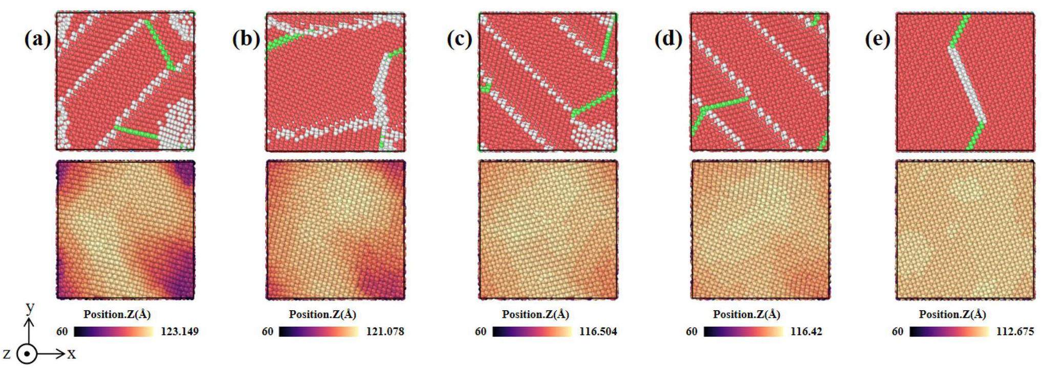
The surface topography of the Ti films at different incident energies was also analyzed, showing that the four surfaces at lower energies (Fig. 8(a–d)) exhibit similar topographies and banded grains, which are oriented along both the (002) and (101) directions. This is due to the earlier occurrence of layer mismatches in the films under low-energy deposition, which leads to incomplete relaxation of the crystal structure. The Ti film deposited at an incident energy of 20 eV in Fig. 8(e) has larger grain sizes compared to those deposited at other energy levels. Moreover, the film deposited at an incident energy of 20 eV exhibits a uniform (101) surface orientation. This suggests that the (101) surface is more favorable than the (002) surface at high temperatures (500 K). This finding is consistent with the findings of Chawla et al. [18].
To further illustrate the effect of the incident energy on the surface quality of the deposited thin films, the surface roughness of the films was evaluated. The surface roughness is a common descriptor of the microscopic morphology of a film, and it affects the film properties to a certain extent. Typically, the lower the surface roughness, the greater the oxidation resistance. As the incident energy increases, the surface roughness also increases, which in turn alters the diffusion paths and nucleation mechanisms of the Ti atoms to some extent. The presence of diverse nucleation sites on high-roughness surfaces results in a more randomized and denser nucleation of the Ti film. Additionally, concave and convex structures on rough surfaces prolong the retention time of the atoms, potentially contributing to the emergence of the 3D island growth mode and influencing the overall quality and homogeneity of the films. In the MD simulations presented in this work, the surface roughness of the film was calculated from the z-coordinate of the atoms on the surface of the film, which is expressed as the root-mean-square roughness R. The surface roughness of the film can be calculated from the z-coordinate of the atoms on the surface of the film as follows [47]:
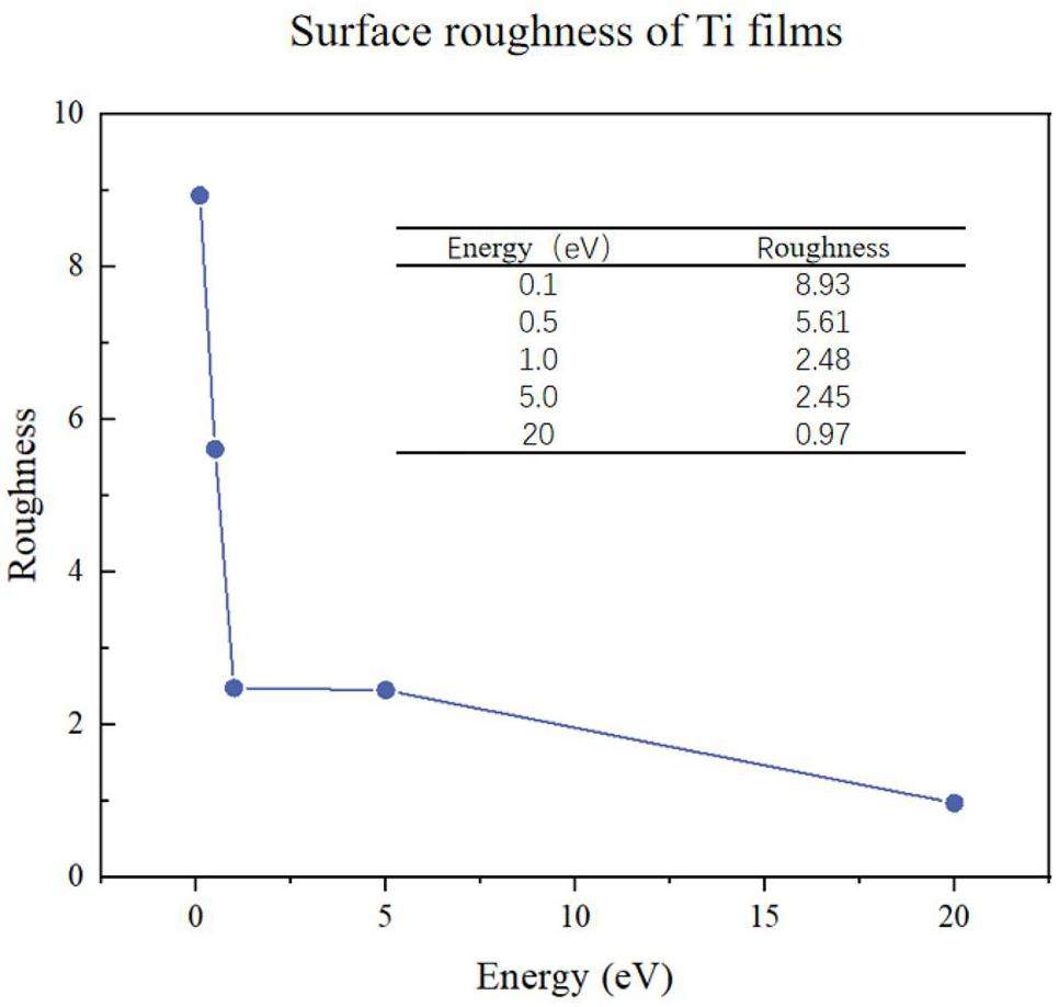
The results demonstrate that the incident atomic energy profoundly influences the final surface roughness of the Ti films. At low incident energies, increasing the energy of the incident atoms has a markedly beneficial effect on the surface roughness of the films. However, this effect becomes less pronounced as the incident energy increases from 0.1 to 5 eV, reaching a plateau. As the incident energy increases to 20 eV, the surface roughness decreases further to 0.97. It is believed that the first decrease in surface roughness is due to the surface diffusion of the Ti atoms during deposition, and the second decrease is the result of grains merging at high energies. The incident energy of the deposited atoms exerts a pronounced influence on the surface roughness of the resulting film. An increase in surface roughness can facilitate the formation of additional sites for tritium adsorption. However, it should be noted that a higher surface roughness also gives rise to the generation of more intricate nucleation sites during the process of film growth. This, in turn, has the potential to influence the intrinsic properties of the film, including its thickness uniformity and grain size. It is therefore hypothesized here that a segmented deposition method can be employed to control the quality of the film by utilizing different incident energies throughout the deposition process.
Ti diffusion behavior on the Si(100) surface
Selective surface orientation is typically observed during the deposition of Ti thin films. Moskovkin et al. [48] revealed that during the deposition process, Ti(002) planes parallel to the substrate are generated in the at low incident energies, whereas (100) planes parallel to the substrate are mainly observed at high incident energies. To investigate the reasons for this phenomenon, deposition simulations were conducted at 300 K and 0.1 eV, and surfaces containing (002) planes without (100) planes were obtained. The results are shown in Fig. 10(a). Unlike the 500 K simulation, no BCC nanocrystals are formed in this simulation. This indicates that the surface orientation of the Ti(100) planes is determined by the BCC nanocrystalline phase transformation, and this transformation process, shown in Fig. 10(c–e), is also consistent with the mechanism of the Ti metal phase transformation [49, 50]. During the phase transition process, the lattice undergoes a large deformation along the β[110] direction. Since the film has a larger relaxation space in the Z-axis direction, the
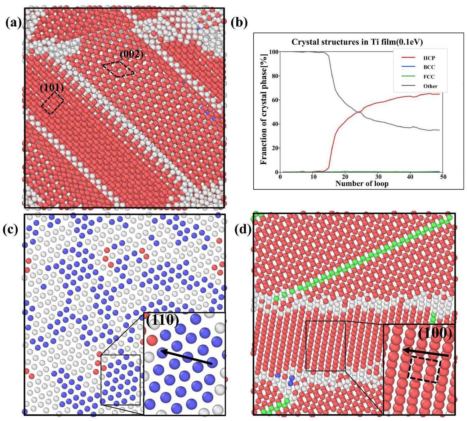
When calculating the surface energy, a truncation energy consistent with that mentioned above was adopted, and the convergence of different layers and different k-points was tested. The final calculation results are shown in Table 3. These results indicate that α(100), as a close-packed surface of HCP-Ti, has a higher surface energy than the other surfaces. It is believed that the lattice deformation induced by the phase transition is the direct cause of the observed selective surface orientation and that the energy stability of the surface is the fundamental cause of the observed selective surface orientation. The ambient temperature during thin-film deposition has an impact on the crystal structure and surface orientation of the resulting film. To enhance the energy conversion efficiency and output power density of tritium cells, it is essential to ensure that the metal films possess a robust crystal structure and an optimal surface orientation, which enable effective tritium adsorption and osmotic diffusion. It must be acknowledged that the tritium adsorption and permeation–diffusion processes are highly complex, and further studies are required to ascertain the full extent of these effects. Our findings demonstrate, however, that experimenters can exert partial control over the crystal structure and surface orientation of Ti metal films by controlling the ambient temperature.
| Surface | Surface energy (J⋅m-2) |
|---|---|
| β(110) | 1.75 |
| α(002) | 1.96 |
| α(100) | 2.03 |
Conclusion
The objective of this work is to investigate the diffusion and deposition behavior of Ti atoms on the Si(100) surface at the atomic scale through the use of atomic-scale simulations. A more realistic surface model than those used in previous studies was employed to calculate the adsorption energies of the Ti atoms at different sites on the Si(100) surface. This enabled the identification of the optimal path for the diffusion of the Ti atoms on the surface. The atomic deposition simulation results indicate that the Ti atoms strongly prefer to cover the entire surface, with this process being regulated by their 2D diffusion. The nucleation of the Ti films is influenced by the upward diffusion of the Si atoms, with the stable HCP grains in the film often accompanied by the presence of FCC laminated dislocations. The surface roughness of the Ti films gradually decreases with increasing incident energy, which is related to the crystal structure transition in the films. From this study, it can be concluded that regulating the incident energy during deposition can effectively control the surface roughness of the Ti films, thereby influencing the thickness uniformity and grain size of the film. In addition, the direct reason for the formation of the (100) surface in the film is the occurrence of lattice deformation during the phase transition of the BCC nanocrystalline material, and the fundamental reason is that the (100) surface itself has a more stable structure. By tuning the ambient temperature during deposition, it is possible to influence the crystal structure and surface orientation of the Ti thin films, which is crucial for enhancing the performance of tritium betavoltaic cells.
Ti/Si interface enabling complementary metal oxide semiconductor compatible, high reliable bonding for inter-die micro-fluidic cooling for future advanced 3D integrated circuit integration
. J. Micromech. Microeng. 30,Growth of Ti-O-Si mixed oxides by reactive ion-beam mixing of Ti/Si interfaces
. J. Phys. D Appl. Phys. 47,Use of Si KLL Auger shifts and the Auger parameter in XPS to distinguish Ti silicides from a Ti/Si mixture in thin films
. J. Electron Spectrosc. Relat. Phenom. 234, 57-63 (2019). https://doi.org/10.1016/j.elspec.2019.04.004Wettability and joining of reaction-bonded silicon carbide (RBSC) by Ti–Si eutectic alloy
. Ceram. Int. 50, 21184-21192 (2024). https://doi.org/10.1016/j.ceramint.2024.03.227Modified graphene by 1 MeV electron irradiation in betavoltaic cell
. Nucl. Instrum. Methods Phys. Res. Sect. B 554,Influence of N2 flow rate on structure and properties of TiBCN films prepared by multi-cathodic arc ion plating and studied with ion beam scattering spectroscopy
. Nucl. Sci. Tech. 28, 59 (2017). https://doi.org/10.1007/s41365-017-0212-0Design and Preparation of SiC Radiation Voltaic Isotope Battery
. At. Energy Sci. Technol. 55, 182 (2021). https://doi.org/10.7538/yzk.2020.youxian.0896 (in Chinese)Review–betavoltaic cell: The past, present, and future
. ECS J. Solid State Sci. Technol. 10,Titanium tritide films as betavoltaic power sources
. J. Electron. Spectrosc. Relat. Phenom. 71, 660-665 (2017). https://doi.org/10.1080/15361055.2017.1290952Long-term stability of betavoltaic battery model and prototype based on tritium/c-silicon PN junction devices
. J. Isot. 34, 10-15 (2021). https://doi.org/10.7538/tws.2021.34.01.0010Initial research in composite electrodes with energy storage applied for betavoltaic isotope battery
. At. Energy Sci. Technol. 52, 175-180 (2018). https://doi.org/10.7538/yzk.2018.52.01.0175 (in Chinese)Effect of different modification methods on the output performance of graphene betavoltaic isotope batteries
. J. Isot. 37, 319-326 (2024). https://doi.org/10.7538/tws.2024.youxian.035Hydrogen isotope effects of Ti, Zr metals
. Fusion Sci. Technol. 60, 1568-1571 (2023). https://doi.org/10.13182/FST11-A12733Properties of Ti and Ti-alloy film deposited by direct current magnetron sputtering
. At. Energy Sci. Technol. 42, 933-937 (2008). https://doi.org/10.7538/yzk.2008.42.10.0933 (in Chinese)Structural and optical property of titanium oxide film prepared by energy filtering magnetron sputtering technique
. Int. J. Appl. Ceram. Technol. 13, 164-169 (2016). https://doi.org/10.1111/ijac.12425Research progress of titanium-based thin films prepared by magnetron sputtering
. Therm. Spray Technol. 12, 17-21 (2020). https://doi.org/10.3969/j.issn.1674-7127.2020.02.003Deposition-rate dependence of orientation growth and crystallization of Ti thin films prepared by magnetron sputtering
. Thin Solid Films 574, 71-77 (2015). https://doi.org/10.1016/j.tsf.2014.10.053Microstructural characterizations of magnetron sputtered Ti films on glass substrate
. J. Mater. Process. Technol. 209, 3444-3451 (2009). https://doi.org/10.1016/j.jmatprotec.2008.08.004Study on process parameters of magnetron sputtering titanium coating in deep porous structures
. ACS Omega. 9, 14551-14557 (2024). https://doi.org/10.1021/acsomega.4c00540Link between plasma properties with morphological, structural and mechanical properties of thin Ti films deposited by high power impulse magnetron sputtering
. ACS Omega 418,Role of the Si–Si bond stability in the first stages of Ti diffusion on a Si(111) 2 × 1 surface. A periodic DFT study
. Appl. Surf. Sci. 273, 496-501 (2013). https://doi.org/10.1016/j.apsusc.2013.02.068Periodic DFT study of Ti deposition on defective Si(100) surfaces
. Appl. Surf. Sci. 335, 160-166 (2015). https://doi.org/10.1016/j.apsusc.2015.02.046Periodic DFT study of Ti deposition on defective Si(100) surfaces
. Surf. Sci. 606, 754-761 (2012). https://doi.org/10.1016/j.susc.2012.01.006Effect of crystalline/amorphous interfaces on thermal transport across confined thin films and superlattices
. J. Appl. Phys. 119, (2016). https://doi.org/10.1063/1.4953683Investigation of interfacial matching between 3C-SiC substrate crystals and its surface layer deposited Cu elements using molecular dynamics simulations
. Surf. Interfaces. 43,A combined molecular dynamics/Monte Carlo simulation of Cu thin film growth on TiN substrates: Illustration of growth mechanisms and comparison with experiments
. Appl. Surf. Sci. 570,Molecular dynamics simulation on the effect of dislocation structures on the retention and distribution of helium ions implanted into silicon
. Nanotechnol. Precis. Eng. 3, 81-87 (2020). https://doi.org/10.1016/j.npe.2020.03.003The mechanism of room-temperature oxidation of a HF-etched Ti3C2Tx MXene determined via environmental transmission electron microscopy and molecular dynamics
. InfoMat 6,Molecular dynamics study of surface binding energy and sputtering in W-V alloys
. Fusion Eng. Des. 195,Molecular dynamics study on the dependence of thermal conductivity on size and strain in GaN nanofilms
. Chin. Phys. B 32,Molecular dynamics simulations of droplet coalescence and impact dynamics on the modified surfaces: A review
. Comput. Mater. Sci. 230,Combining molecular dynamics with Monte Carlo simulations: implementations and applications
. Theor. Chem. Acc. 132, 277-288 (2013). https://doi.org/10.1007/s00214-012-1320-xOn the time scale associated with Monte Carlo simulations
. J. Chem. Phys. 141,Molecular dynamics and Monte Carlo simulations in the grand canonical ensemble: Local versus global control
. J. Chem. Phys. 98, 4897-4908 (1993). https://doi.org/10.1063/1.464945Growth and properties of Cu thin film deposited on Si(001) substrate: A molecular dynamics simulation study
. Appl. Surf. Sci. 261, 690-696 (2012). https://doi.org/10.1016/j.apsusc.2012.08.082Molecular dynamic simulation for Cu cluster deposition on Si substrate
. Comput. Mater. Sci. 56, 85-94 (2012). https://doi.org/10.1016/j.commatsci.2012.01.010Projector augmented-wave method
. Phys. Rev. B 50, 17953 (1994). https://doi.org/10.1103/PhysRevB.50.17953Special points for Brillouin-zone integrations
. Phys. Rev. B 13, 5188 (1976). https://doi.org/10.1103/PhysRevB.13.5188Fast parallel algorithms for short-range molecular dynamics
. J. Comput. Phys. 117, 1-19 (1995). https://doi.org/10.1006/jcph.1995.1039Bond-order potentials for the Ti3AlC2 and Ti3SiC2 MAX phases
. Phys. Rev. B. 100,Development of an interatomic potential for the simulation of defects, plasticity, and phase transformations in titanium
. J. Chem. Phys. 145,A silicon powder diffraction standard reference material
. J. Appl. Cryst. 8, 45-48 (1975). https://doi.org/10.1107/S0021889875009508Mechanical properties of nano Ti films with different thickness
. J. Mater. Eng. 43, 50-56 (2015). https://doi.org/10.11868/j.issn.1001-4381.2015.11.009Formation of the Co/Si(111)7x7 interface: AES- and EELS-study
. Appl. Surf. Sci. 166, 125-159 (2000). https://doi.org/10.1016/s0169-4332(00)00393-7Effects of deposition parameters on structures of sputtered Ti films and TiO2 nanotube arrays prepared by anodic oxidation
. Rare Metal. Mater. Eng. 37, 2186-2190 (2008). https://doi.org/10.3321/j.issn:1002-185X.2008.12.027Kinetic energy-induced growth regimes of nanocolumnar Ti thin films deposited by evaporation and magnetron sputtering
. Nanotechnology 30,Simulation of molecular dynamics associated with surface roughness on an Al thin film
. Surf. Coat. Technol. 203, 918-921 (2008). https://doi.org/10.1016/j.surfcoat.2008.08.011Link between plasma properties with morphological, structural and mechanical properties of thin Ti films deposited by high power impulse magnetron sputtering
. Surf. Coat. Technol. 418,Variant selection of grain boundary α by special prior β grain boundaries in titanium alloys
. Acta Mater. 75, 156-166 (2014). https://doi.org/10.1016/j.actamat.2014.05.003Crystallographic variant selection in Ti-6Al-4V
. Acta Mater. 52, 5215-5224. (2004). https://doi.org/10.1016/j.actamat.2004.07.034The authors declare that they have no competing interests.

