Introduction
When a particle passes through a matter, it induces ionization or excitation. If the particle is charged, its electromagnetic field interacts directly with the orbital electrons of the atoms in the matter. In the case of γ-ray or X-ray, it first goes through some intermediate processes to produce the Photoelectric effect, the Compton effect, or Electron pairs, which transfer some or all of the energy to the orbital electrons of the atom in the matter and then produce ionization or excitation. In the case of uncharged neutral particles, such as neutrons, charged particles are produced by nuclear reactions, which then cause ionization or excitation. Elements that use the ionizing effect, luminescence phenomenon, and physical or chemical changes caused by nuclear radiation in gases, liquids, or solids for nuclear radiation detection are called nuclear detectors. The nuclear detectors use the appropriate detection medium as the matter that interacts with the particles, and the ionization or excitation generated by the particles in the detection medium is transformed into various forms of signals. Nuclear electronics reads and processes the signal from the nuclear detectors and extracts the information. This information can then be used to determine parameters directly or indirectly of the nuclear radiation, such as the type, energy, intensity, arrival time or lifetime.
More than 100 types of radiation detectors can give electrical signals. Gas detectors were introduced as early as 1908 [1]. However, it was not until 1931 that the problem of fast counting was solved after the advent of pulse counters [2]. In 1947, scintillation counters appeared, significantly improving the efficiency of detecting particles due to their much greater density than gases [3]. The most notable is the NaI (Tl) scintillator, which has a high energy resolution for γ rays [4]. In the early 60s, the successful development of semiconductor detectors led to a new development of energy spectrum measurement technology. Modern nuclear detectors used in high-energy physics, nuclear physics, and other scientific and technological fields have been rapidly developed over the last few decades. This paper will discuss the principle, short history, development, and recent advances on some representing semiconductor detectors, gaseous detectors, scintillation detectors, Cherenkov detectors, transition radiation detectors, and readout techniques.
Semiconductor Detectors
When the radiation ray or particles incident into the sensitive region of the semiconductor detector, the radiation ray or particles continuously loses energy and generates electron-hole pairs, and is separated from the two ends of the electrode drift under the action of the external electric field to collect, thus forming an output pulse signal. According to the structure classification, the structure of semiconductor detector has crystal conductivity type, p-n junction type, p-i-n junction type, Schottky junction type and so on.
The number of electron holes created is related to the energy of absorbed particles or rays and the energy of electron-space pair formation, shown in the following formula:
Silicon Detectors
Silicon detectors are very well suited to detecting and measuring ionizing radiation and light caused by interacting with charged particles and photons (Soft X-rays). A great feature of silicon detectors is that they can operate with low noise at room temperature due to the band gap of 1.12 eV. In addition, silicon has a high density of 2.329 g/cm3, a small average ionization energy of 3.62 eV, good mechanical stability, and is easy to produce on a large scale. These advantages make silicon the perfect option for many physics experiments and equipment.
1960 Bromley showed a proposal for a 3D array of silicon diodes that would function as a solid-state "cloud chamber" [5]. The Charge-Coupled Device (CCD), introduced in 1969, with good spatial resolution and low noise in photon detection, received the Nobel Prize in 2009. Since the first half of the 1980s, Silicon Strip Detectors (SSD) have become dominant in particle tracking [6]. In the 1980s and 1990s, an evolution started from strip to pixel detectors, mainly consisting of monolithic and hybrid types. The Low Gain Avalanche Diode (LGAD) recently provided fast detection of Minimum Ionizing Particles (MIPs) with a timing resolution of several picoseconds. Recent decades have witnessed substantial growth in silicon detectors, expanding from a few thousand channels to billion channels with dramatically increased granularity facilitated by rapid advancements in semiconductor technology [7].
Charge-Coupled Device
CCD comprises a series of coupled Metal-Oxide-Semiconductor (MOS) capacitors as its fundamental structure. Electrons are produced when photons hit MOS capacitors because of the photoelectric effect, and will be collected as signal charge packets by potential wells of each MOS capacitor, which are formed by applying positive voltages to gate electrodes. Subsequently, the packets stored in each MOS capacitor are transferred from one pixel to its neighbor through sequential adjusting gate voltages of each MOS capacitor. The last capacitor dumps its charge into a charge amplifier, which converts the charge into a voltage, and then readout. MOS capacitors share readout circuit, so the transferring process will be repeated continuously until all the signal charge packets are read out.
CCD-based detectors can be implemented in several different architectures. The most common are full-frame, frame-transfer, and interline. In a full-frame device, all of the imaging area is active. While in frame-transfer CCDs, half of the silicon area is covered by an opaque mask, typically aluminum. It is necessary to quickly transfer input signals from the image area to the opaque or storage area to minimize smear in this design. Unlike frame-transfer, the interline architecture involves only a pixel shift from the imaging area to the storage area, enabling shutter times of less than 1 μs and virtually eliminating smear.
The advantages of CCD are apparent. It has excellent spatial resolution because its pixel size can be very small. Pixels as small as 1.56 μm × 1.56 μm have appeared as early as 2006. Also, the CCD has low noise because its readout process does not produce noise, making it well-suited for small signal detection. In addition, shared readout provides good pixel-to-pixel consistency. What’s more, it’s worth noting that modern CCD technology allows for manufacturing large wafer-level devices, simplifying the mechanical design of detectors, which is crucial for experiments requiring a large sensitive area [8].
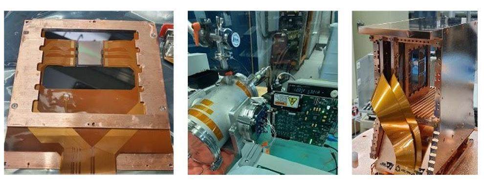
The primary utilization of CCD is in astronomical observation. For instance, the Skipper-CCD, designed for the Oscura experiment [9] and employed in low-energy neutrino studies and dark matter searches, is crafted from high-resistance (HR) n-type silicon wafers. The sensor has a thickness of 675 µm, an effective area of 1.9 cm × 1.6 cm, and charge can be read through amplifiers at the four corners. Meeting the Oscura’s stringent requirements, including a readout time of less than 2 hours and a radioactive background rate of 0.01 event/kg/day/keV, the sensor exhibits a dark current of approximately 10-6 e-/pix/day. Test results conducted at Fermilab (as depicted in Fig. 1) reveal that 71% of the sensors exhibit sub-electron noise, with a surface dark current of about 0.031 e-/pix/day [9].
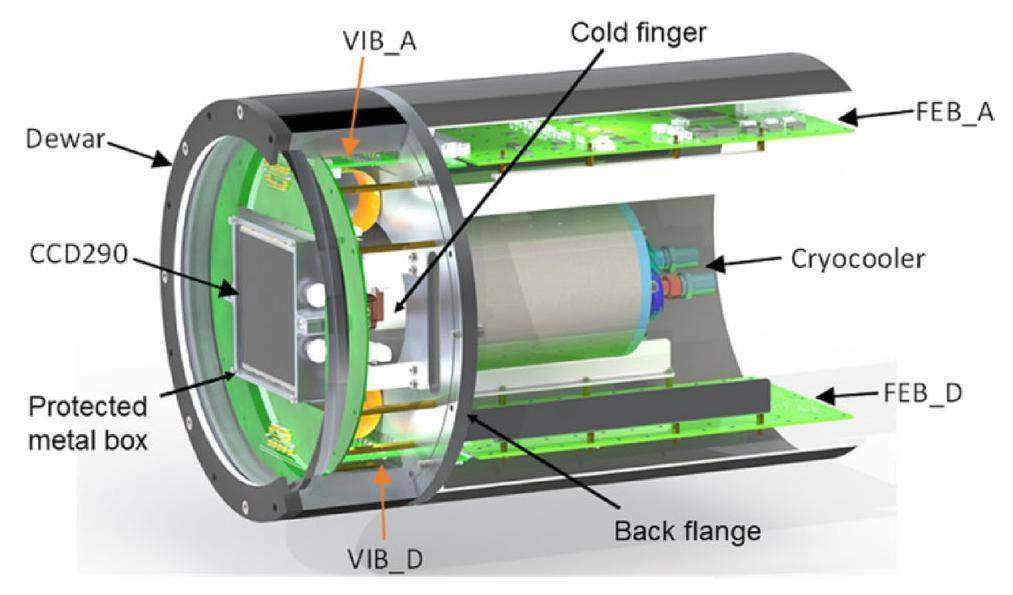
The "Mozi" Wide Field Survey Telescope (WFST) is a new generation survey telescope that is being built in China. It is equipped with a mosaic CCD camera with 0.73 gigapixels on the primary focal plane for high quality image capture over a 6.5-square-degree field of view [10]. Comprising nine E2V CCD290-99 chips, each with a resolution of 9 K × 9 K and a pixel size of 10 µm, the camera supports full-frame or split full-frame readout modes. The 3D model of the CCD detector system is illustrated in Fig. 2. The readout can occur through 8 or 16 output channels, with a typical readout noise of 4 e-@0.5MHz. To meet the scientific objective of rapid sky surveying, the maximum readout speed reaches 3 MHz, and the readout noise is maintained below 15 e-@1MHz [11]. Nowadays, CCD also finds applications in fields such as spectral analysis and heavy ion Computed Tomography (CT) [12].
Silicon Strip Detector
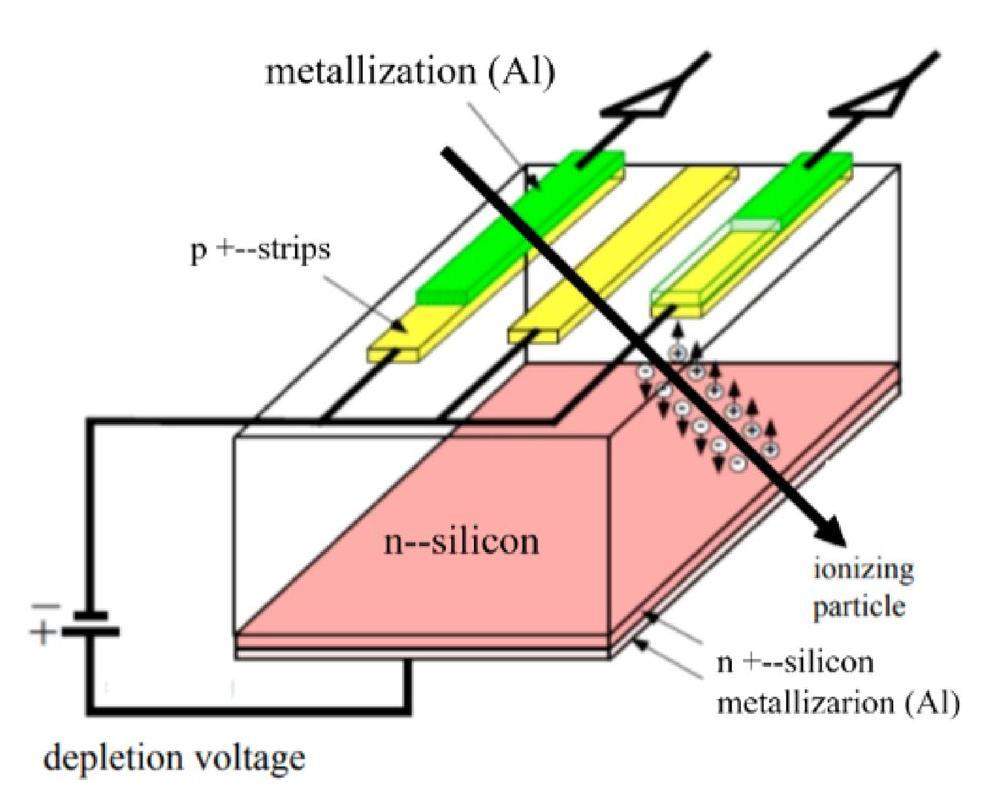
The SSD is the first detector device using the lithographic capabilities of microelectronics, mainly used as a vertex and tracking detector. As shown in Fig. 3, the SSD is commonly fabricated through selective etching of microstrips on the surface of N-type silicon wafers. The highly doped P+ microstrip forms a PN junction on the surface and extends its depletion layer across the entire N-type substrate with applied reverse bias voltage. After covering aluminum on the top, a microstrip that acts as a charge-collecting electrode is completed. Multiple strips form a single-sided SSD, which provides one-dimensional position detection. When particle hits, electron-hole pairs are generated in the depletion region because ionization caused by deposited energy. Electrons, driven by an external electric field, are collected by the strips, converted into electrical signals, and processed by the readout circuit. The double-sided SSD featuring heavily doped P+ junction strips that collect the electrons and the N+ ohmic strips that collect holes can realize two-dimensional position detection. Since SSDs have low noise, good linearity, a high count rate, and excellent position and energy resolution, they are widely used in high-energy physics, nuclear physics, and space detection facilities [13, 14].
In high-energy physics, the radiation-hardened Silicon Microstrip Vertex Detector (SVX’) was incorporated into the CDF experiment during the Tevatron
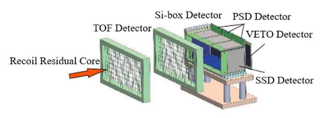
SSD plays a vital role in nuclear physics experiments. The Institute of Modern Physics (IMP) has constructed a gas-filled recoil separator called Spectrometer for Heavy Atom and Nuclear Structure (SHANS) to study the heavy and superheavy nuclei properties. A silicon semiconductor detector box (Si-box) is installed at the focal plane position of the separator, as illustrated in Fig. 4. The Si-box incorporates three Position Sensitive Silicon Detectors (PSSD) at the back as implantation detectors, with a thickness of 300 μm and a collective effective area of 150 mm × 50 mm, offering 3 mm horizontal position resolution. The PSSD demonstrates a typical energy resolution of 50 keV FWHM for 5–10 MeV α particles. Leveraging this PSSD detector, it can be used to measure α particles of 1–20 MeV, implantation and fission fragments with energies of 5–200 MeV, and detect the escaping radioactive decay events [22]. Similar applications of SSD in nuclear physics can also be found in MUST, TIARA, and HIRFL-RIBLL. The MUST ("MUr à Strips") detector consists of 8 SSD–Si (Li) telescopes used to identify recoiling light charged particles through time of flight, energy loss and energy measurements and to determine precisely their scattering angle through X and Y position measurements [23]. The Transfer and Inelastic All-angle Reaction Array (TIARA) consists of 8 resistive charge division detectors forming an octagonal barrel around the target and a set of double-sided silicon-strip annular detectors positioned at each end of the barrel, designed to study direct reactions induced by radioactive beams in inverse kinematics [24]. The detection system consists of five Δ E - E telescopes, consisting of one double sided silicon strip detector (DSSD) as the Δ E detector, and a square silicon detector as the E detector, designed to measure the angular distributions of both elastic scattering and breakup simultaneously, on the Radioactive lon Beam Line in Lanzhou at Heavy lon Research Facility in Lanzhou(HIRFL-RIBLL) [25].
The SSD has been a "standard" component for space detection [27]. The Dark Matter Particle Explorer (DAMPE), launched in 2015, incorporates silicon-tungsten tracker-converter (STK) to collect the electron-positron pairs converted from the incoming photons by the tungsten converters. As shown in Fig. 5, the STK contains of 6 tracking planes each consisting of 2 layers of SSD arranged orthogonally. Each single layer consists of 16 ladders, and each ladder comprises 4 modules bonded end-to-end. The SSDs are glued on the flex part of the Tracker Front-end Hybrid (TFH) board to form a ladder. Each layer of SSD has an active area of 0.55 m2, with a total radiation length of 0.976% X0, spatial resolution < 80 μm within 60 incidence, and a total weight of 154.8 kg.

The readout is performed on one every other strip (corresponding to 384 channels per ladder) in the SSD. The signal shaping and amplification is performed by six VA140 ASIC chips mounted on the TFH[28]. The VA140 is a 64-channel low-noise charge-sensitive amplifier ASIC from the Norwegian IDEAS company. Each channel of the VA140 comprises a charge-sensitive preamplifier, a filter shaping circuit, and a sample and hold circuit. The input charge dynamic range spans from -200 fC to 200 fC, with a shaping time of only 6.5 μs. This ASIC employs serial readout through a multiplexing circuit and the power consumption is 0.29 mW/channel.
Based on the successful development and operation of China’s first DAMPE, the Purple Mountain Observatory of the CAS, together with several institutions, proposed the Very Large Area Gamma-ray Space Telescope (VLAST).As shown in Fig. 6, the VLAST plans to use SSD to build Silicon Tracker and low Energy gamma-ray Detector (STED). The main function is to realize the conversion of high-energy gamma photon-electron pairs, and to achieve high-angular resolution observation of gamma photons through the track measurement of electron pairs. The main technical indicators of STED are [29]:
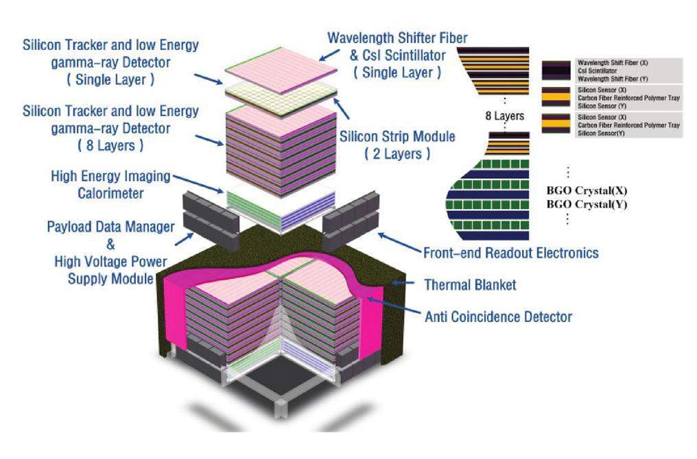
• Number of detector layers: 8 super layers; (each super layer includes a CsI detection layer and two large silicon micro-strip detection layers);
• Active detection area of each layer: ≥ 2.8 m × 2.8 m;
• Detection energy range: 1 MeV –100 MeV;
• Spatial resolution < 0.1 (@50 GeV).
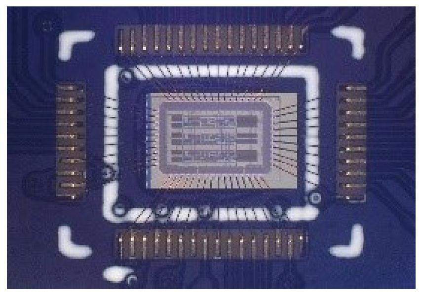
The VA140 from IDEAS company is also a potential candidate for the readout of the SSD on VLAST. In addition, the IMP is now developing a readout chip called SiReadout. The first version of the chip is shown in Fig. 7. The preliminary single-channel test indicates that it has a gain of 2.01 mV/fC, power consumption of approximately 220 μW, a peaking time of 3.12 μs, linearity error below 1%, and an Equivalent Noise Charge (ENC) of 992 e- at zero F plus 13.5 e- per pF.
Also, the ALPHA Magnetic Spectro-meter (AMS) experiment similarly utilizes SSD to build a magnetic spectrometer to measure momenta, charges and mass of the particles [30], the Fermi Large Area Telescope (Fermi-LAT) builds the LAT tracker to reconstruct the incoming photon direction, etc [31].
Silicon Pixel Detector
Silicon pixel detector is currently one of the main detectors and is expected to play a significant role in the future due to their exceptional spatial resolution, reduced material budget, low noise, and rapid readout rates. It mainly consists of a densely packed pixel array and peripheral readout circuits, with each pixel containing a charge-sensitive unit for collecting electrons and outputting electrical signals and its front-end signal processing circuit. The distinct signals generated by particles interacting with different pixels offer precise two-dimensional positional information. Silicon pixel detectors can be classified architecturally into monolithic and hybrid types.
Monolithic Active Pixel Sensor The monolithic type integrates the charge-sensitive unit and front-end circuit on a single substrate, minimizing complexities in interface designs. This integration ensures high granularity, a low material budget, and a relatively small equivalent input capacitance. Monolithic Active Pixel Sensor (MAPS) is currently one of the most promising and well-developed technologies among monolithic types.
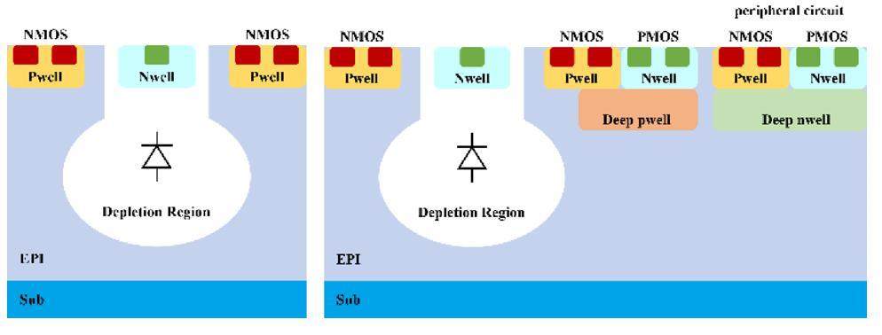
MAPS shares the similar detection principle as SSD. As depicted in Fig. 8, a lightly doped P-type epitaxial (EPI) layer grows on a substrate heavily doped with P-type impurities, the Nwell/P-EPI diode is the charge-sensitive unit and the front-end circuit is also on the same substrate connecting to it directly. MAPS typically features pixel sizes ranging from 10–30 μm, resulting in a position resolution of 3–7 μm. The readout speed can achieve hundreds of kilohertz, and noise is maintained at approximately 10e- level. MAPS demonstrates a good balance in resolution, material budget, radiation hardness, readout speed, and power consumption.

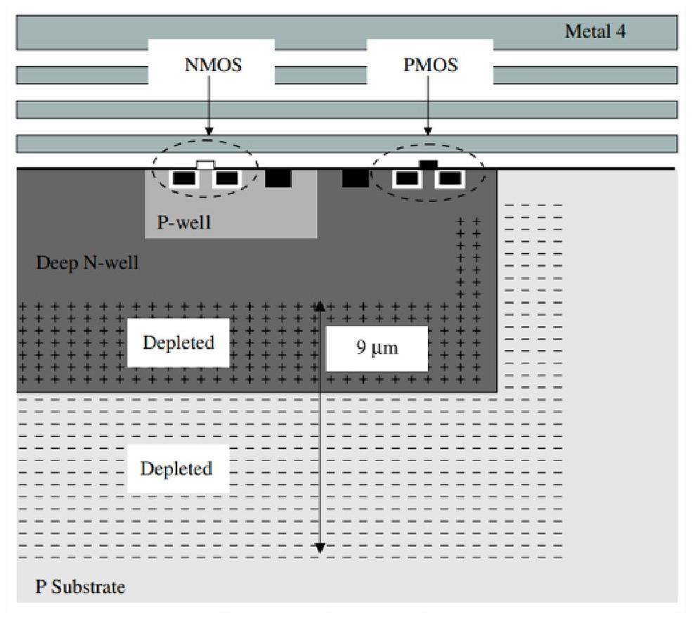
The EPI process in MAPS significantly impacts charge collection. The standard EPI process has a thickness of approximately 10 μm which causes a small depletion layer, and an electrical resistivity of around 10 Ω cm, making thermal diffusion the dominant way for charge collection. Therefore, it needs a long time to collect electrons and the collection efficiency is very low. In contrast to that is an HR EPI process with a thickness of up to 40 μm and an electrical resistivity that potentially can reach ∼1000 Ω cm. The depletion layer is thicker, and charges can also be collected by drifting. The process of collecting is faster and more efficient. Moreover, it reduces the probability of electron-hole pair recombination, enhancing radiation hardness and improving the Signal-to-Noise Ratio (SNR). In the standard twin-well process (Fig. 9 left), PMOS cannot be used in pixel design because the Nwell where PMOS resides competes with the Nwell of the diode, leading to a reduction in Charge Collection Efficiency (CCE). Hence, the deep Pwell is needed to isolate the two. In addition, applying a reverse bias voltage to the substrate could expand the depletion layer region which means increasing CCE and improving radiation hardness, but it may also cause the peripheral readout circuit on the same substrate not to work properly, so deep Nwell is needed for protection. Simulations can give the preliminary study of charge collection in certain process for specific particles in the early phase of design [32-34]. In summary, the prevailing approach for MAPS involves the utilization of a complete quadra-well process (Fig. 9 right) with HR EPI.
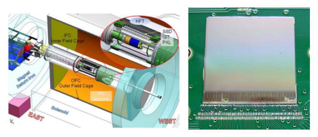
In experimental physics, MAPS finds primary applications as vertex and track detectors in collider experiments. The Heavy Flavor Tracker (HFT) detector in the STAR experiment is the world’s first detector to use MAPS to enhance vertex resolution and extend measurement capabilities in the heavy flavor domain [35]. The HFT detector incorporates MAPS in its innermost two layers (at radii of 2.8 and 8 cm from the beamline) among four concentric cylinders near the STAR interaction point, and these layers feature 400 Ultimate (MIMOSA-28) chips, covering a total silicon area of 0.16 m2, as illustrated in Fig. 10. Every layer costs a global material budget of only 0.5% X0 because the chip on it operates normally with air cooling at room temperature[36].
The Ultimate chip, designed by the IPHC, fabricated by 0.35 μm HR OPTO process (400 Ω cm), features a pixel array of 928 × 960 pixels with a pixel pitch of 20.7 μm, providing a sensitive area of approximately 3.8 cm2. Its pixel includes a sensing diode for charge collection as well as an amplification circuit and a Correlated Double Sampling (CDS) circuit for signal extraction and noise removal. Each pixel column is terminated with a high precision discriminator and is read out in a rolling shutter mode at 5 MHz. The discriminator’s outputs are processed through an integrated zero suppression logic and the sparsified data are sent out to the acquisition via two 160 Mbps LVDS outputs. The Ultimate demonstrated a MIPs detection efficiency near to 100%, a fake hit rate of less than 104, and power consumption maintained at 150 mW/cm2[37].
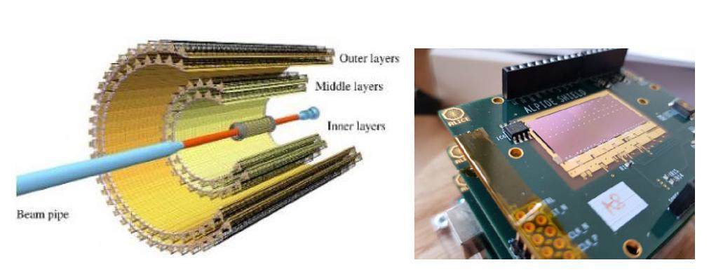
The ALICE Inner Tracking System 2 (ITS2) stands as the world’s largest detection system employing MAPS. As illustrated in Fig. 11 left, the detector layout features concentric 7 layers with radii ranging from 23 mm to 400 mm. These layers consist of over 24120 ALICE Pixel Detector (ALPIDE) chips (Fig. 11 right) [38], forming a 10 m2 active detection area with a total of 12.5 × 109 pixels.
ALPIDE is fabricated using the TowerJazz 180 nm quadra-well HR CMOS process (>1 kΩ cm), and features 512 × 1024 pixels with the pitch of 28 μm, providing a sensitive area of 30 mm × 13.8 mm [41]. Its pixel includes an octagon collection diode which achieves nearly 100% CCE and a distinctive front-end circuit consisting of a continuously active discriminating amplifier and a multiple-event memory, which yields an ENC of less than 10 e-. The in-pixel multiple-event memory is read out asynchronously through a priority encoder circuit in each double column. This is fast and power efficient as the expected occupancy is low and only hit pixels are read out in a hit-driven mode. Data is collected at the periphery and shipped off the detector by means of a high-speed serial link [42]. Extensive beam tests confirm that ALPIDE achieves a detection efficiency exceeding 99%, a false hit probability below the required 10-6 level, and a spatial resolution better than the desired 5 μm. Even after exposure to a TID of 2.7 Mrad and a non-ionizing energy loss (NIEL) flux of 1.7×10¹³ 1 MeV neq/cm2, surpassing the anticipated detector lifetime, it sustains performance and provides a readout rate of 100 kHz with a power density of less than 40 mW/cm2 [43].
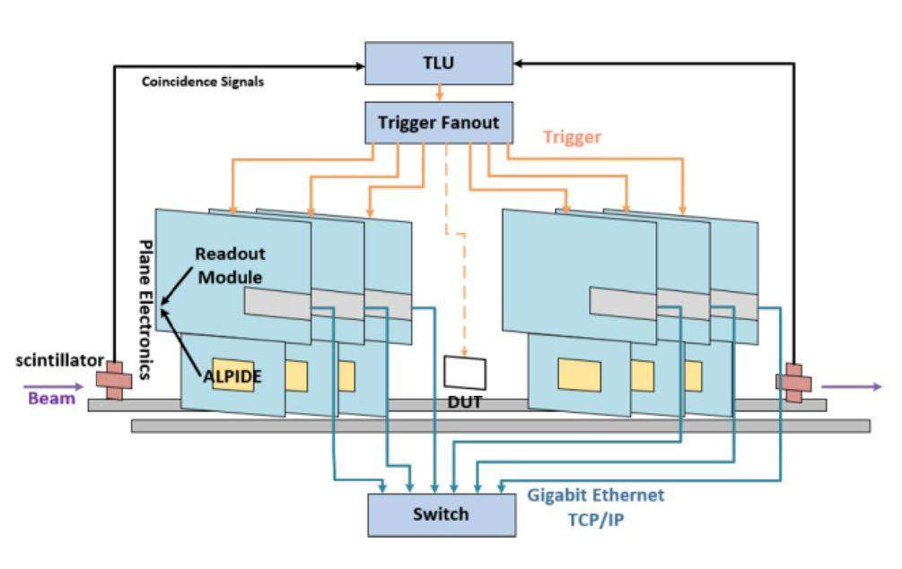
MAPS also plays a crucial role in high-resolution beam telescopes for tracking charged particles, exemplified by the Desy II beam telescope. The first generation adopted the EUDET-type framework, employing MIMOSA-26, which provided outstanding spatial resolution and a lower material budget. Achieving a distribution resolution of 1.83 μm for a 6 GeV electron or positron beam on the Device Under Test (DUT), the rolling shutter readout operated at a frequency of approximately 10k frames per second. As MIMOSA-26 production ceased and updating became unfeasible, a new beam telescope was constructed based on ALPIDE technology (Fig. 12). This telescope features a sensitive area of 414 mm2, a trigger rate of up to 100 kHz, and significantly reduced noise levels compared to the previous telescope. This enhancement allows for more efficient beam utilization and a cleaner tracking environment. The spatial resolution remains in the micron range (approximately 5 μm at 6 GeV), with a low fake hit rate [44].
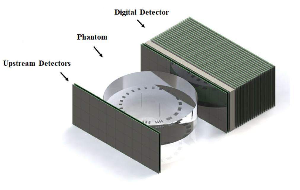
MAPS is increasingly pivotal in proton and heavy-ion imaging, particularly in the burgeoning field of ion beam radiotherapy. Unlike traditional photon radiation, ion beams exhibit a Bragg peak, a concentrated dose deposition, whose depth can be finely adjusted by altering the beam energy. This feature enhances protection for healthy tissues [45]. Proton and heavy-ion imaging research contributes to refining treatment plans for proton/heavy-ion therapy [46]. Current methods of making particle therapy treatment plans rely on converting X-ray CT HU value into Relative Stopping Power (RSP) of proton/heavy ions, which led to inevitable range uncertainties. However, the Bergen proton CT (PCT) system (Fig. 13), incorporating a Digital Tracking Calorimeter (DTC), can directly measure the RSP to address this problem.
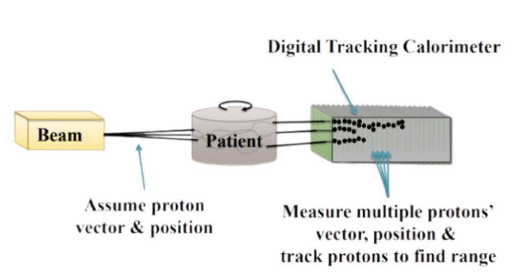
The DTC comprises 43 layers, each equipped with 108 ALPIDE chips, which feature the first two layers as tracking layers for acquiring the position information of incoming particles and the subsequent 41 layers as a digital calorimeter. As a particle traverses the detector, it deposits energy in the sensitive layer, generating a 3D digital hit map along its path. The final prototype has a measuring area of 27 × 16.6 cm2, which is adequate for imaging the human head [47].
Another compact full digital system that utilizes the MAPS with a similar structure to Bergen PCT but for heavy-ion imaging is the Hi’CT proposed by IMP (Fig. 14). The simulation results achieve less than 1% deviation in Relative Stopping Power (RSP) and better image quality of CATPHAN phantoms. The real-time imaging capability of Hi’CT may reduce target deviations caused by organ or respiratory movement, achieving optimized treatment effectiveness and improved quality of life for patients [48].
MAPS technology has advanced with the adoption of stitching technique in wafer-level chip manufacturing. The stitching technique is the way to continue the scaling of technology in the semiconductor industry because of the reticle size limitation [49]. It is achieved by dividing the reticle into sections that could individually be exposed and aligned with neighboring sections [50]. As Fig. 15 left shows, the design reticle gets subdivided in sub-frames that correspond to sub-frames of the photomasks. During the photolithographic patterning of wafers, these are selectively exposed to adjacent locations according to a pre-established pattern. This requires very accurate translations and alignment of the wafers between each exposure. The peripheral structures along the outer edges of the core array and at the four corners are designed in dedicated sub-frames of the reticle. The red lines in the figure indicate the dicing lanes. With a judicious design of the geometries in the reticle sub-frames, large chips with diagonals approaching the wafer diameter become feasible, provided their core area can be constructed as an array of sub-units regularly repeating in space. Interconnections across the sub-units are made with the joining of wiring geometries at the abutment boundaries [51].
The upgrade of ALICE’s ITS3 (Fig. 15 right) is prepared to utilize stitching technology to manufacture a kind of single MAPS on a 12-inch silicon wafer, achieving dimensions of 27 cm × 9 cm. ITS3 is expected to significantly reduce the material budget from 0.35%X0 to 0.05%X0 because the new MAPS will be capable of self-bending without the need for complex support and cooling systems. Simultaneously, ITS3 can place the innermost layer at a radial distance of only 18 mm from the interaction point. These features will enhance the resolution of impact parameters to twice that of all momenta and significantly improve tracking efficiency at low transverse momentum [52]. In addition, large scientific facilities such as the Electron-Ion Collider in China (EicC), the Electron-Ion Collider (EIC), and the Nuclotron-based Ion Collider Facility (NICA) are also preparing to adopt wafer-scale MAPS implemented with stitching technology.
As mentioned before, reverse bias can enlarge the depletion layer region, but normal CMOS processes typically have a maximum bias substrate voltage of 5 V [53]. High voltage (HV) CMOS technology is starting to be used in MAPS to improve sensor properties. Unlike the quadra-well process mentioned earlier, in the HV CMOS process, the deep Nwell is used to protect the entire circuit except for the charge-sensitive unit, which is another kind of diode composed of EPI and the deep Nwell itself as shown in Fig. 16. Such a design can even achieve a 100% fill-factor [54]. A typical example is ALTASpix3,originally designed for the upgrade of the ATLAS tracking experiment and a option for the silicon tracking detector of the Circular Electron Positron Collider (CEPC). Its deep Nwell connects to the positive power supply rail at 1.8 V and the maximum voltage of the substrate is around 66 V, corresponding to a depleted region of approximately 30 μm [55].
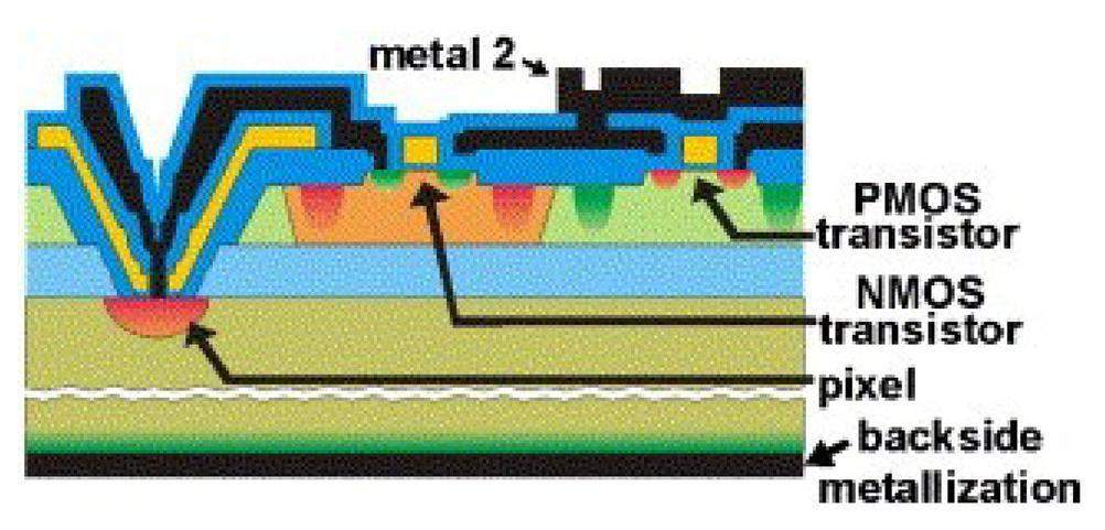
The Silicon-On-Insulator (SOI) CMOS technology has also been used to significantly enhance radiation hardness for MAPS design. SOI wafers are composed of a thin Silicon film (device layer) on top of an insulating layer (buried oxide) that is manufactured on a standard Silicon substrate. In traditional SOI technologies, the substrate serves solely as a mechanical support for the silicon film. In detector applications, as shown in Fig. 17, the substrate has high resistivity and is utilized for creating the sensor (a matrix of fully depleted diodes) monolithically coupled to the readout electronics integrated in the silicon film above the insulating layer [56]. Laboratory laser testing of SOI CMOS pixel detectors has demonstrated excellent TID tolerance up to 1 Gray [57].
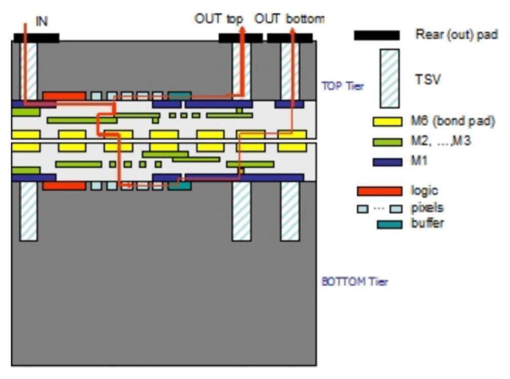
One consideration to address limitations in pixel size is constructing circuit chips in three-dimensional (3D) structures [58]. One method is 3D stacking, illustrated in Fig. 18, employing Through-Si Via (TSV) for vertical communication.
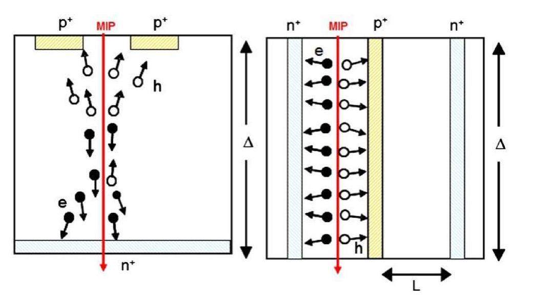
Another method, known as 3D detectors, decouples electrode distance and substrate thickness. It allows to place the electrodes perpendicular to the silicon wafer penetrating through the substrate. Therefore, in contrast to standard planar detectors, the depletion region laterally grows between the electrodes [60], as depicted in Fig. 19.
Nuclear physics experiments also require MAPS to have the capability for time and energy measurements beyond position only. Time measurement is needed to address the high counting rate requirements, such as the China Hyper-Nuclear Spectrometer (CHNS) and precise monitoring of heavy ion beams, which may require counting rates as high as 106 to 108 counts per second, corresponding to a time precision of 10 ns to 1 μs. Energy measurement contributes to position resolution and particle identification. For example, the Bρ-DE-TOF (magnetic rigidity-ionization energy loss-time of flight) method, which combines momentum generated by trajectory curvature and the Bethe-Bloch formula, is mainly used in the identification of particles in medium to high energy radioactive beams and the identification of reaction products on secondary targets. According to the relationship between ionization energy loss Δ E and particle charge number Z, and velocity v:
MAPS development in China started in the 2010s and has grown rapidly. The representing ones for MIPs detection are the MIC series [64] from Central China Normal University (CCNU), the Taichupix [65] and Jadepix [66] from the Institute of High Energy Physics (IHEP) of the CAS, the SuPix from Shandong University [67], etc. The domestic MAPS with multi-dimensional measurement for nuclear physics includes the Nupix [68, 69] from the Insitute of Modern Physics (IMP) of the CAS, and the Topmetal-M [70] from IMP and CCNU, both designed with China’s own CMOS process.
Hybrid Hybrid pixel detectors feature the charge-sensitive unit and front-end readout circuit on separate substrates connected by flip-chip bonding. The hybrid pixel detectors can use different materials for the charge-sensitive unit and readout circuit, which can be optimized separately. For example, the GaAs, CdTe, and other non-silicon materials are used for the sensor part in X-ray imaging, and the readout part is designed with silicon [6]. The simplified design of the charge-sensitive unit also enables good yields at larger sizes. Therefore, hybrids generally offer flexible readout capabilities and broader applications compared to MAPS. However, the complex and labor-intensive production process and numerous production steps make hybrid pixel detectors relatively more costly [57].
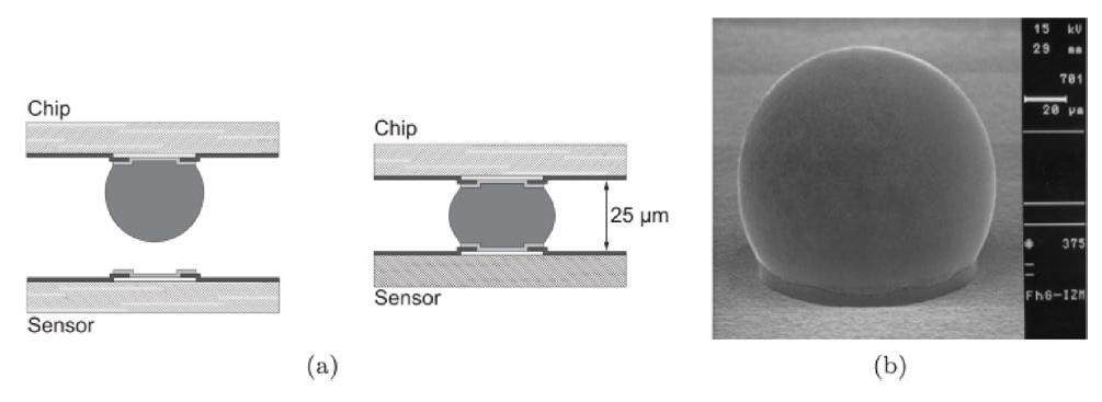
The reliability and excellence of the flip-chip bonding techniques significantly impact overall chip performance. The solder bumps and bonding technique is the most commonly used (Fig. 20). Before producing the solder bumps, the sensor and chip surfaces undergo treatments, such as cleaning and de-oxidizing. After accurately locating the devices to be connected, the solder is heated to melt and then cooled to form a strong connection. IBM introduced solder balls in the C4 (Controlled Collapse Chip Connection) process in 1969. However, the bumps’ pitch limit of 170 μm or greater is often too large for fine-pitch and high-granularity pixel detectors in particle physics. Eutectic solder bumps are considered to be the primary soldering technology for hybrid pixel detectors, with high connection density of as low as 25 μm and bump sizes of 15 μm. Higher yields can be achieved using Sn/Pb and lead-free Sn/Ag or Au/Sn alloys, and the final pitch limit is around 5–10 μm. Eutectic solder bumps have been used to realize hybrid pixel detectors in ATLAS, achieving high bonding rates of more than 99%. Other technologies include In-In bonding, Cu-Cu direct bonding, oxide-oxide direct bonding, and Solid-Liquid Interdiffusion (SLID) bonding. Overall, bonding technology requires adding small capacitance to pixel preamplifiers through bonding connections, good yield and defect rate of less than (open or shorted), good contact (<100 mΩ), and robustness to temperature cycling (-40 ℃ to +60 ℃) [71].
Hybrid pixel detectors have been widely used in collider physics experiments as vertex and track detectors. The first hybrid pixel detector was developed in the RD19 project WA97 particle physics experiment. The hybrid pixel detector has a 64 × 96 pixel array, with a sensitive area size of 53 mm × 4.73 mm and a thickness of 300 μm. Six Omega2 readout chips, each one containing 16 × 64 front-end circuits, are bump-bonded to one pixel array. Each pixel is connected to a virtual ground via a front-end circuit by a Pb-Sn solder bump with a diameter of 38 μm. Each front-end circuit contains a low noise amplifier followed by a comparator with an adjustable threshold (from 4000 to 15000 e-), an adjustable delay line (from 100 ns to 1 μs), and some coincidence and memory elements, which store the bit indicating a particle hit during the time frame selected using an external strobe signal. During the proton run of WA97 in November 1993, the intrinsic precision of the pixels was about 24 μm, and the efficiency of good chips was 98–99%, while the average efficiency of the entire detector (including bad areas) was about 80% [72]. Subsequently, from 1998 to 2006, the hybrid pixel detectors were installed in the four experiments (ALICE, ATLAS, LHCb, and CMS) at CERN.
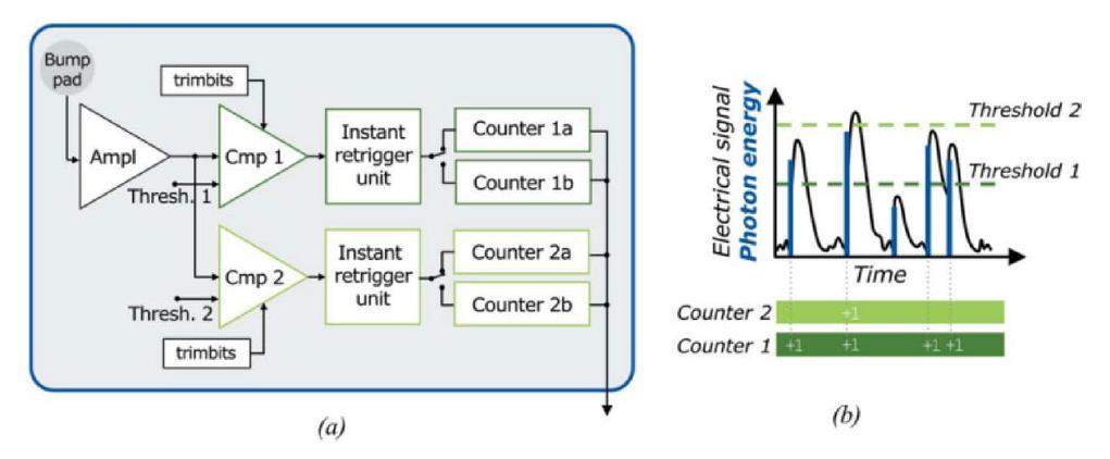
In recent years, hybrid pixel detectors have seen further development in synchrotron experimental facilities, primarily for Hybrid Photon Counting (HPC). Since the initial concept validation for synchrotron sources in 1999, HPC has had a profound impact on nearly all X-ray applications in synchrotrons and laboratories, significantly affecting data quality, data collection speed, and the development of complex data acquisition schemes. A recent example is the EIGER2 readout chip, with a pixel size of 75 μm × 75 μm and an array size of 256 × 256, featuring an amplifier and two energy discriminators (Fig. 21). It has four functionalities: a 8-bit readout mode that doubles the maximum frame rate, a dual-gating mode for parallel measurements of two time-delays in pump-probe experiments, a multi-image stream mode and a line region of interest (lines-ROI) mode with a high frame rate of up to 98 kHz. The charge-sensitive unit that goes with it can be Si or CdTe for photon energies of 3.5–40 keV and 8–100 keV. Since 2018, EIGER2 has been used in the production of various detectors. In the field of macromolecular crystallography (MX), they have been used to employ high-energy X-rays for reducing radiation damage, and in the biomedical imaging field, they are used to advance scanning techniques [73].
The High Energy Photon Source (HEPS) in Beijing also needs a photon counting pixel detector and here comes the HEPS-BPIX series. The HEPS-BPIX chip is a dedicated pixel readout chip that operates in single photon counting mode for X-rays. Fabricated by SMIC 0.13 μm process, it contains a 104 × 72 matrix of 150 μm square pixels. Bump bonded with a 300 μm thick silicon charge-sensitive unit, the measurement results showed that noise after bonding was 115.8 e- rms, the threshold dispersion was 55.1 e- rms after calibration and trimming, and the frame rate was 1.2 kHz with a negligible dead time of 175 ns per frame at 20 MHz clock frequency. All the performance was found to satisfy the project’s requirement [74].
Hybrid pixel detector technology has been widely adopted in various scientific fields, such as medical X-ray imaging, synchrotron radiation applications, low-energy electron microscopy, materials analysis using X-ray diffraction, adaptive optics, dosimetry, and space dosimetry [75]. The Medipix and Timepix series, developed at CERN, are the most common hybrid pixel detectors applied in medical imaging.
The Medipix is primarily used for X-ray photon counting. The latest iteration, Medipix4, is designed to facilitate large-scale applications utilizing high-z materials to achieve high rates (up to 5 × 10⁸ photons/mm2/s) at fine spacing [76]. Medipix4 can be tiled on all 4 sides, making it ideal for building large-area detectors with minimal dead zones, and it is characterized by energy grouping of individual photons while maintaining spectral accuracy by implementing an inter-pixel architecture that corrects for the effects of charge sharing. The Medipix4 chip has three modes of operation: High Dynamic Range Mode (HDRM), Low Noise Mode (LNM), and Ultra-Fast Mode (UFM). In HDRM, the chip can use a CdTe sensor to process X-ray photons with energies up to 154 keV [77]. In LNM, with a fine-pitch configuration without charge-sharing correction, the measured electronic noise is 72 e- rms [78]. In UFM, the front-end’s post-layout analog count-rate capability is 19 × 106 photons/mm2/s [77]. The chip can read out charge-sensitive units with 320 × 320 pixels measuring 75 μm × 75 μm (Fine Pitch Mode, FPM) or 160 × 160 pixels measuring 150 μm × 150 μm (Spectral Mode, SM). The Medipix ASICs have been applied in X-ray CT, prototype systems for digital mammography, CT imagers for mammography, and beta and gamma radiation autoradiography of biological samples. In addition, they can also be used for commercial X-ray material analysis [79].
The Timepix, introduced as a development based on the Medipix2 chip in 2005, addresses the demand for high-resolution time measurement scenarios. It operates in three modes: the hit counting mode, which tallies signals exceeding the threshold, incrementing the count for each signal; the Time of Arrival (ToA) mode, where the counter starts when the signal arrives and stops when the signal ends; the Time over Threshold (ToT) mode, during which the counter tallies the duration the signal exceeds the threshold. The latest Timepix4 is a 24.7 mm × 30.0 mm hybrid pixel detector readout chip with a 448 × 512 pixel array, specifically designed for tiling the detector on all four sides, and can count incoming hits at rates maximum of up to 5 GHz/mm2/s. The block diagram of the Timepix4 pixel cell and super pixel architecture is shown in Fig. 22 [80]. The chip can read out charge-sensitive units at a pitch of 55 μm.
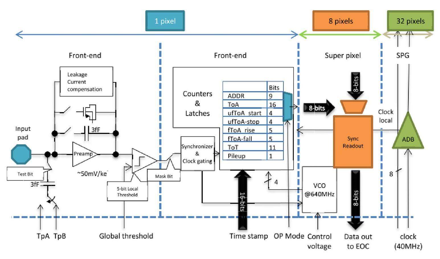
In addition, the Topmetal [70], designed by Central China Normal University, and the IMPix series [81], currently in development at the IMP, are also hybrid pixel readout chips developed by Chinese researchers. It’s worth noting that these chips can also directly collect charge with their exposed topmost metal layer, which can be used for TPCs [70].
Low Gain Avalanche Diode
The high luminosity physics experiments increase the number of collisions in each bunch crosses dramatically. The LGAD, invented by the Centro Nacional de Microelectronica (CNM), Barcelona, Spain, with the support of the CERN-RD50 community [82], can provide a time resolution better than 40 ps and becomes an excellent choice of solid-state timing detectors [83]. Combined with the 3D position information, LGAD-based detectors are considered suitable for tracking.
As an innovative charge-sensitive unit, LGAD enables rapid measurements of MIPs combined with the readout circuit. Its fundamental principle leverages the avalanche gain effect to enhance the sensitivity and resolution. As shown in Fig. 23, an n+/p/p- junction is created along the center of the LGAD’s electrodes. With a reverse bias voltage, a high electric field region is generated in the junction region, which can lead to a multiplication of electrons reaching the n+ electrode. The p-type multiplication layer is to enhance the electric field in that region, and its impurity profile adjusts the gain [84].
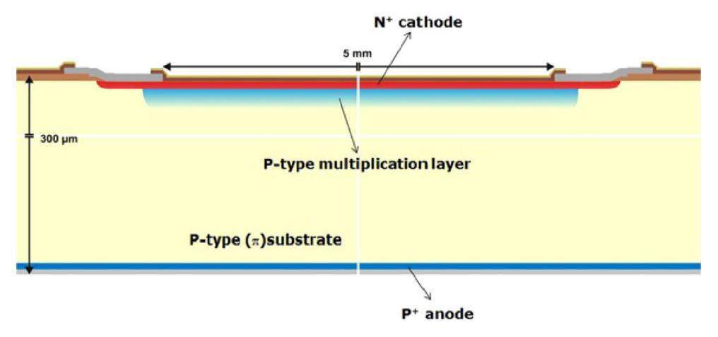
An incident particle to junction generates many carriers, which are then accelerated by an electric field, producing additional secondary carriers, culminating in an avalanche effect that yields a substantial charge signal. By controlling the doping of the P-type multiplier layer, an appropriate multiplication of around 10 allows the fabrication of thinner devices with the same output signal of standard thick substrates [84], which means a decrease in noise and better SNR. On the other hand, the signal shape is mainly governed by the holes escaping toward the backside. Hence, the LGAD with thin active thickness makes the signal rise faster and the collection time shorter [85]. Better SNR means more negligible time jitter and faster signals mean smaller time walks. Therefore, a very high time resolution is achievable.
This LGAD technology has become an emerging detector for physics experiments. The High Granularity Timing Detector (HGTD) based on LGAD [86] from IHEP is a crucial component of the ATLAS phase II upgrade to cope with the extremely high pile-up. This HGTD detector is located in the gap region between the end-cap calorimeter and the cylinder, covering a pseudo-fastness range of 2.4
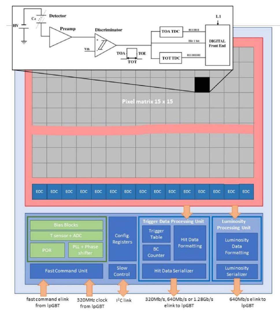
It is also expected to use LGAD to upgrade the internal layers of the CMS detector to optimize the detection performance of energetic particles. In the EiC and EicC projects, LGAD is also under consideration for developing new detectors.
One of the most significant drawbacks of LGADs is their poor spatial resolution. A development trend is using capacitively coupled LGAD (AC-LGAD) to address the dead zone issue at the pixel boundary of LGADs. This technology can achieve a spatial resolution of less than 10 μm. Other silicon detectors based on LGADs, such as deep-junction LGAD (DJ-LGAD) and trench-isolated LGAD (TI-LGAD), are also under development [82].
All Silicon Tracker
Recently, all trackers become a hot topic. This approach usually utilizes a radially compact structure, leaving more space for external particle identification (PID) detectors [87]. It also offers faster readout speed and significantly reduces the workload for calibration and alignment. Additionally, it can provide a higher resolution of momentum and single-track.
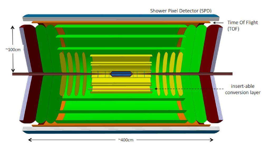
The ALICE collaboration has proposed an all-silicon tracker capable of covering the rapidity region |η| < 4 [88]. The detector concept comprises a barrel and two end caps constructed from layers of ultra-thin Si-sensors. As shown in Fig. 25, this all-silicon tracker includes the Inner Tracker (IT), outer tracker (OT), Time-Of-Flight (TOF) detector, and electromagnetic Shower Pixel Detector (SPD). The inner tracker comprises 3 layers within the beam pipe and 4 disks at both ends. It will employ wafer-level ultra-thin CMOS MAPS, manufactured using the stitching technique mentioned earlier, with 10 μm × 10 μm pixels providing better than 3 μm position resolution, with a material budget of 0.05% X0 per layer. The outer tracker has 7 layers and 6 disks at each end, utilizing the same technology as the vertex detector. The pixel size is increased to 30 μm × 30 μm to reduce power density, yielding a spatial resolution of about 5 μm and a material budget of 0.5% X0 per layer. The TOF detector is planned to be a silicon detector with a temporal resolution of 20 ps, based on LGAD. It is utilized for identifying hadrons and electrons at very low transverse momentum (pT < 500 MeV/c). Additionally, the SPD can identify electrons and photons (pT > 500 MeV/c) with a disk at each end. In summary, with unprecedented low mass, the all-silicon tracker would allow reaching down to an ultrasoft region of phase space, to measure the production of very-low transverse momentum lepton pairs, photons and hadrons at the LHC [88].
Meanwhile, the Electron-Ion Collider (EiC) plans to construct a fully silicon-based tracking detector, projected to be 242 cm long and 43.2 cm in radius. As shown in Fig. 26, six layers will provide tracker coverage for low values of pseudorapidity. They are laid out in three double layers to provide redundancy, and the middle double layer is placed equidistantly between the inner and outer double layers to measure hits in the vicinity of the sagitta to optimize the momentum resolution. In addition, five disks in each direction provide coverage at larger absolute values of pseudorapidity. With the current configuration, the material budget they contributed is less than 5% X0. This geometry was implemented in GEANT4 and studied within the full Monte-Carlo framework for detector simulation. Preliminary results show that the design meets the physics requirements over the entire 0<p 30 GeV/c range for -2.0 < η < 3.0 at a 3.0 T field [87]. Furthermore, fully silicon-based detectors have also been proposed for the CHNS and EicC.

Wide Bandgap Semiconductor Detector
In general, the reverse leakage current increases with the increase of temperature, and when the temperature of the silicon detector exceeds 50 ℃, the leakage current is very large, which limits the application in extreme conditions.
The intrinsic carrier concentration of thermal excitation can be defined as electron concentration
The SiC Detector
Among the wide bandgap semiconductor materials, silicon carbide material has better quality and the most mature device technology, so that SiC radiation detector has a great development. There are more than 200 isomers in SiC crystals, and the C/Si atoms in each isomer are stacked in a different order. The three most common isomers are 3C-SiC, 4H-SiC and 6H-SiC, and the number before H represents the number of C/Si atomic layers in the stacking cycle. In the above various types of SiC, usually 4H-SiC is the most one in the common application [90].
The wide bandgap semiconductor material SiC has a wide bandgap with 3.26 eV at room temperature and has good radiation resistance. With extremely high breakdown voltage characteristics, this device can withstand high voltage and high current density. The saturation velocity of electron can improve the charge response speed of the detector. At the same time, it has high thermal conductivity, which is three times that of Si, and it has good heat dissipation properties and stable chemical properties. The device has the characteristics of high resistivity and small dark current. Especially in the three materials of gallium nitride, silicon carbide and diamond, SiC can obtain larger crystal size (6 inch and 8 inch), so SiC radiation detector is also the most deeply studied detector in the wide bandgap semiconductor.
The research of charged particle detector of silicon carbide can be traced back to the 1950s, and the neutron detector of silicon carbide was reported as early as 1957 [89]. In 1973, V.A. Tikhomirova et al. used a silicon carbide device as a fission fragment counter at a high injection rate (4 × 10¹⁴n/cm2), and compared with the silicon detector, it is confirmed that the silicon carbide device has good radiation hard characteristics [91]. However, in the next 20 years or so, due to the limitation of growing process technology, the quality of SiC material is relatively poor, which makes the research progress of SiC radiation detector is very slow.
Until the late 1990s, researches carried out a lot of fruitful research work, significantly reduced the defects (such as dislocation, microtubule, etc.) produced in the growth process of SiC crystals, and at the same time, the controllable doping process has also been significantly improved, which makes the manufacturing technology of high-performance SiC devices have been developed by leap. In 1997, F.H. Ruddy’s research team of Westinghouse Electric developed two SiC detectors, SBD and PN junction, with the energy resolution of 5.8% and 6.6% for α particles, respectively, and no effect on the performance of the detector in the temperature range of 22–89 ℃ [92]. With the continuous development and improvement of SiC thin film epitaxial growth technology, the research team reported the results of high energy resolution in 2006. The SBD detector with the epitaxial thickness of 100 μm was prepared, and the energy resolution of 5.449 MeV α particles reached 0.37% [93]. In 2012, the United States, a team of scientists at the university of South Carolina were compared the performance of the detector of an insulator SiC with n-type epitaxial layer on single-crystal SiC, the results show that the performance of the epitaxial film detector is better than single crystal detector performance, n-type epitaxial detector on the best bias is 100 V, to 5.486 MeV alpha particle energy resolution was 2.7%, within the scope of soft X-ray also have very good response. In 2015, B. Zat ’ko’s team at the Slovak Academy of Sciences reduced the epitaxial layer doping concentration to 1.0 × 1014 cm-3, 15 nm Ni/Au (0.3 mm) was used as a Schottky electrode, the leakage current of the detector is only 2 pA at the reverse voltage of 700 V, and the energy resolution of 5.486 MeV α particles reaches 0.25%, which is one of the best reported result [94].
Heavy particle identification in nuclear physics experiments, there are Italian c. Ciampi and s. Tudiso researchers such as more than 40 scientific research personnel of SiCILIA (Silicon Carbide Detectors for Intense Luminosity Investigations and Applications) related research report of the project, they are based on 10 mm and 100 mm thick SiC telescope structure Δ E - E detector, The feasibility of SiC detector for particle identification under high fluence was verified [95]. In addition, proton beam monitoring in laser plasma experiments [96], α particle diagnosis in nuclear fusion [97] also have important applications. In addition, in recent years, some complex SiC detectors, such as SiC microstrip detectors, have been developed for the identification of heavily charged particles and isotopes [98].
Neutron detection technology has a wide application prospect in many fields such as space radiation environment detection, contraband detection, scientific experiment, medicine, military and industry [99, 100]. Experiments show that the SiC detector in proton 1.4 × 10¹⁶ p/cm2 and 7 × 10¹⁵ n/cm2 can still be work [101, 102]. In silicon carbide, 12C and 28Si can react with fast neutrons to release α particles, which interact with SiC to generate electron hole pairs, this can be applied to detect fast neutrons [103]. However, since the neutron reaction cross section 12C and 28Si is small, so SiC neutron detector generally uses solid neutron conversion layer material, such as 10B, 6Li and its composite materials, which convert neutrons into charged particles for detection. At the same time, appropriate transfer layer thickness should be simulated to achieve the best detection efficiency. Usually SiC detectors use a flat structure, only part of the charged particles incident into the semiconductor is detected, so the efficiency is very low, usually no more than 5% [104].
Due to the deep penetration of X and γ rays, a thickness sensitive zone of several hundred microns is needed. The device with epitaxial thin sensitive zone can only detect low energy and X and γ-rays [105-107]. In order to realize high-energy ray detection, the quality of the bulk single crystal used needs to be improved, and the energy spectrum test is difficult. However, in synchrotron radiation, SiC detectors are also used in X-ray energy detection and beam monitoring [108]. The semi-insulating bulk 4H-SiC detector shows moderate resolution of γ ray spectra, and the 4H-SiC n-type epitaxial layer detector shows good resolution of 59.5 keV γ-ray spectra.
In addition, with the development of device technology, the 3D structure which can be used for ultra-fast detection and the micro-structure silicon carbide detector which can be used for efficient neutron detection have also become an inevitable demand [109]. These studies are bound to facilitate ultrafast radiation testing with silicon carbide detectors at high fluence [110], in-core monitoring [111], neutron monitoring of space nuclear reactor power supply, fusion [97], free electron laser [112] and so on.
The GaN Detector
Gallium nitride is a direct bandgap semiconductor with a hexagonal wurzite structure (α-GaN). GaN thin films are usually grown on non-primary substrates, i.e., heteroepitaxy. Considering the lattice constant, crystal structure, chemical, thermal and electrical properties of the material, silicon, sapphire (Al2O3) and SiC are the most popular substrates [113]. However, due to the mismatch between lattice and thermal expansion coefficient, there is still a high dislocation density in GaN on heterogeneous substrate (108 – 1010 cm-2).
GaN thin film growth techniques are varied. The most used techniques are metal organic chemical vapor deposition (MOCVD) and molecular beam epitaxy (MBE). MBE has the advantages of precise process control, low growth temperature and low working pressure. However, the growth rate of GaN in MBE is relatively slow and the operation cost is high [114], so it is mostly confined to laboratory research. MOCVD, especially in combination with the epitaxial transverse overgrowth technique (ELOG), can produce high quality GaN films, for example, in some studies, the linear dislocation density can be reduced to 105 –107 cm-2 [115, 116]. In addition, the high throughput capability of MOCVD also determines its extensive application in commercial large-scale GaN epitaxy growth [114]. At the same time, hydride vapor phase epitaxy (HVPE) is the main technology for the production of thick GaN wafers due to its high growth rate (hundreds of microns per hour) [116]. The dislocation density decreases with the increase of GaN thickness [117]. Therefore, the thick GaN grown by HVPE has higher crystal mass and lower impurity concentration; for example, Xu et al. were able to produce less than 1 × 106 cm-2 of thick GaN dislocation density. However, HVPE is difficult to achieve controlled film doping and low background carrier concentration (about 1014/cm3) without compensation, and is rarely used to prepare GaN pin thin film devices.
GaN doping has a certain effect on the performance of the detector [118]. Undoped GaN usually exhibits n-type characteristics due to unintentional background doping, such as silicon and oxygen. These impurities can be released from the reaction chamber, usually produced by quartz, and act as shallow donors in GaN [116]. In addition, some donor point defects in GaN, such as nitrogen vacancies, are also responsible for the n-type conductivity of undoped GaN [116, 119].
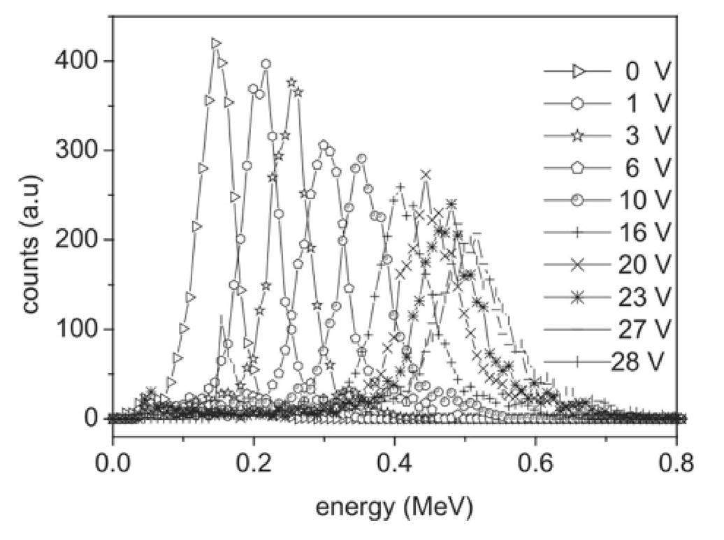
The first GaN α-particles realized by Vaitkus et al. are based on this device structure[120]. MOCVD method was used in Al2O3 The N-GaN epitaxial layer grows 2 µm continuously on the surface, and Au acts as the Schottky contact surface, forming a double Schottky structure. The detector is detected in the reverse bias range of 0 ∼ 28 V (breakdown voltage is 29 V). The charge collection efficiency (CCE) of 5.48 MeV alpha particles emitted by 214AM source was measured to close to 100%, as shown in Fig 27. This work proves that GaN devices can be used in particle detection. The double Schottky structure is simple to manufacture and does not need to optimize the ohmic contact, but the long distance between the two Schottky contacts leads to parasitic capacitance and resistance affecting the performance of the detector [121].
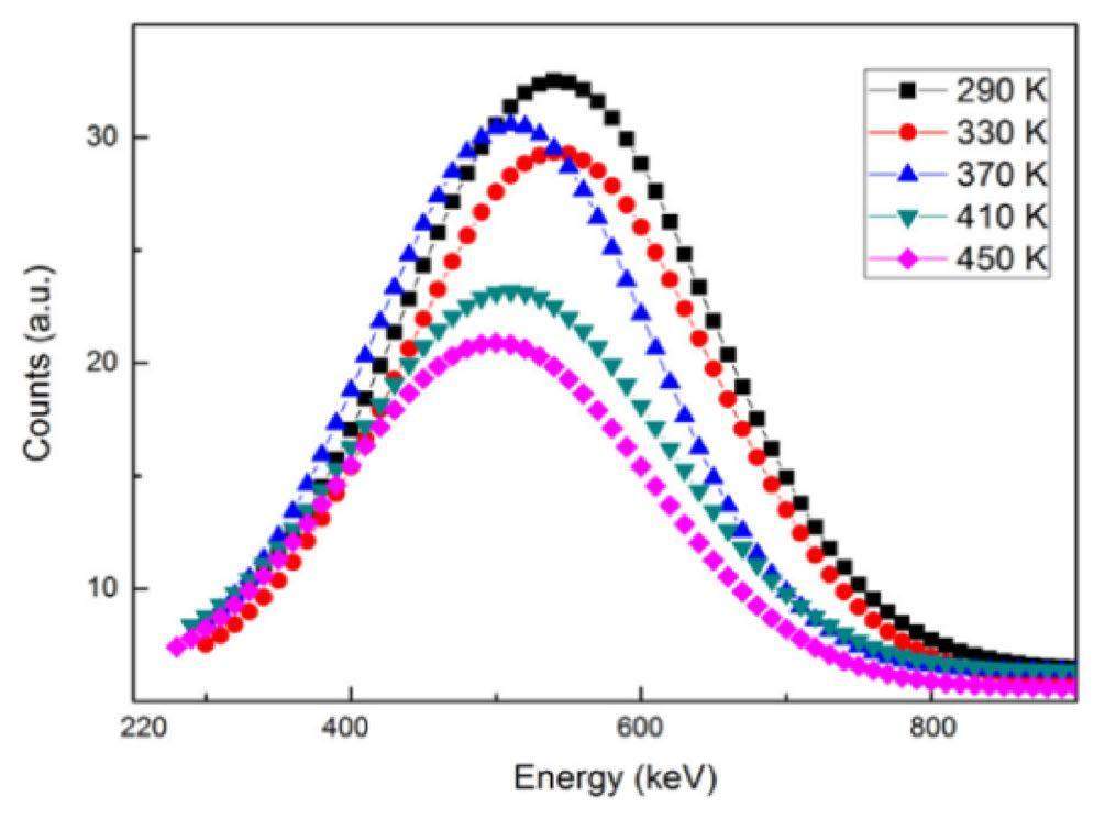
Compared with GaN Schottky devices, PIN devices have more lower leakage current. Lu et al. applied this structure to α particle detection in 2012[122]. At -30 V operating voltage, the reverse leakage current of the detector is in the nA range, and the pulse height spectrum of 241Am alpha particles is measured. The CCE at this voltage is about 80%, but the energy resolution (FWHM) is about 40%. The authors attribute this high energy resolution to the thick dead layer and the absence of a collimator. In addition, Zhu et al. studied the radiation performance of GaN α particle detector with temperature variation based on the thin film p-i-n structure [123]. As the temperature changes from 290 to 490 K, the peak position of 241Am Alpha particle pulse height spectrum is slightly shifted towards the lower energy direction, and the change of half peak width is almost negligible, as shown in Fig. 28. This work proves that GaN-based alpha particle detector has good stability in high temperature environment.
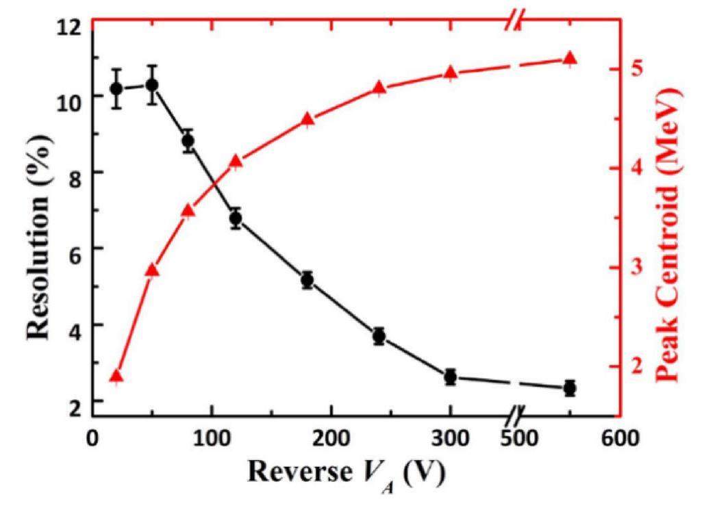
Grant et al. proposed the application of bulk GaN to nuclear radiation detection in 2005 [124]. The bulk GaN Schottky structure detector developed by Xu et al. has the lower leakage current (7.53 ± 0.3 nA at -200 V) and the highest operating voltage (550 V) among all GaN α-particle detectors reported. Due to the high operating voltage and low background carrier concentration, the depletion width can reach 27 mm at -550 V, and the energy resolution can be improved to 2.2% [125], as shown in Fig. 29. Sandupatla et al. also applied this structure to particle detection. Metal-organic gas phase epitaxy (MOVPE) method was used to grow the sensitive zone with a thickness of 15 μm, compensated by Mg impuries, and the carrier concentration was as low as 7 × 1014 cm-3. High CCE (65%) can be obtained at low voltage (-20 V) and also observed at -300 V (96.7%) [126].
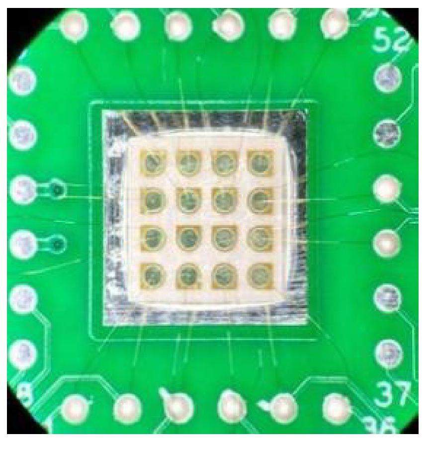
Recently, Liang et al. have done a lot of work on sapphire based GaN pin detectors, and simulated and optimized the performance of GaN pin devices [127, 127].GaN pin detectors with 10 μm and 20 μm thickness sensitive zones were realized by means of isoelectron doping process. The leakage of 10 μm detector at reverse 40 V is 10 pA, and the leakage at reverse 200 V bias is only 10 nA. using the hybrid 241Am and 239Pu α source was tested, and the energy resolution reached about 3%. The actual device is shown in Fig. 30.
It has also been noted that GaN detectors can be used for X-ray detection because of their high radiation resistance and insensitivity to visible light. Duboz et al. firstly studied the absorption coefficient of GaN to 6 ∼ 40 keV photon energy. The large absorption coefficients observed between 10 keV and 20 keV indicate that GaN is difficult to use for detecting X-rays with photon energies greater than 20 keV, except that GaN layers are very thick, such as GaN substrates [129]. Due to the thin epitaxial layer, X-ray spectroscopy measurement based on GaN detectors still has great challenges.
The application of GaN in particle detection shows its great potential in the field of neutron detection. However, research on GaN neutron detectors is still in its infancy. Detecting neutrons with GaN detector is mainly to cover the detector with neutron transfer layer material, and to detect neutrons indirectly by detecting the α particles emitted after the interaction between neutrons and transfer layer. The commonly used neutron transfer layer material is containing 6Li and 10B of material. When a neutron is absorbed by the transfer layer, two charged particles are produced, thus achieving neutron detection. However, the detection efficiency of this method is still affected by the long neutron mean free path and the neutron mean free path [121] Limits on the short distances at which charged particles are produced in a detector. Gd (thermal neutron capture cross section 49000 Barns) is also used to doping GaN in order to obtain high detection efficiency [130, 131].
The Diamond Detector
Diamond detectors have a lot of research in radiation detection, especially detection of alpha particles, X-rays and neutrons. In terms of energy resolution, Iwona Wodniak et al. used 2.5 mm × 2.5 mm × 50 μm diamond single crystals to make X-ray detectors with a maximum half-width of 21 keV and a minimum energy resolution of 0.36%, comparable to that of silicon detectors [132]. A. V. Krasilnikov et al. developed three kinds of spectral determination systems based on natural diamond detectors, and measured D-T neutron spectrum and flux on the tokamak fusion test reactor [133]. D-T neutrons pass through 12C (n, α)9Be reaction interacts with the natural diamond detectors reaction and produces a narrow peak in the pulse height distribution, with an energy resolution of 2% ∼ 3%, which is well isolated ∼ 2 MeV from other reactions. L. Giacomelli et al. show that the energy resolution of 20 MeV incident neutrons is 1%, and the detection efficiency is 1%, which opens up a new prospect for the study of fast ion physics in high-energy fusion devices, such as the S-D neutron spectrum of deuterium-tritium plasma heated by neutral beam injection [134].
In recent years, diamond thin film detectors, especially CVD diamond polycrystalline and single crystalline thin film detectors, have been widely studied. Due to the difficulty of preparation and high cost, there are few reports on the research of high quality thick single crystal diamond. For low energy α-rays and X-rays, complete deposition can be achieved in diamond films of tens of micron. However, for the detection of high-energy rays, such as X-rays of 10 keV, diamond films of dozens of microns can only deposit about 3% of their total energy, and even diamonds of 200 ∼ 300 μm thickness can only deposit about 15%.
The diamond nuclear radiation detector has good energy resolution. In a large energy range, the amplitude of the pulse signal is proportional to the energy of the incident particle. The high radiation resistance makes the detector particularly suitable for neutron measurement; Diamond material detector has a long lifetime, especially suitable for strong radiation environment particle testing. The main problem of diamond detector is the material preparation of large size and low cost. On this basis, further studies are needed on n-type doping, Ohmic and Schottky contacts and micromachining processes. In addition, in the aspect of signal processing, how to identify particles is also a problem.
The Ga2O3 And BN Detector
Compared with the SiC, Ga2O3 and BN detectors are still relatively immature. This is mainly due to the lack of breakthrough in the growth technology of Ga2O3 with high quality and low background carrier concentration. The advantages of both detectors are a wide bandgap and the ability to be largely free of interference except for the longer wavelength of the UVC, making it possible to work on the ground even in daylight. We have made some progress in the particle detector of Ga2O3 alpha detector, using HVPE technology to grow high-quality gallium oxide epitaxial layer, and realize the particle detector on the surface of the earth to resist light interference.
Hexagonal boron nitride (h-BN) is the simplest Group III nitride semiconductor material, with a 10B percentage content of about 20%, 10B (n, α) reaction cross-section in the thermal neutron energy region of about 3840 barns, theoretically can achieve 100% thermal neutron capture rate. Neutron detection can be realized by using charged particles generated by interaction with neutrons to excite electron hole pairs. It has many advantages such as high energy resolution, high charge collection rate and good sensitivity, and is the most ideal material for direct thermal neutron detection. h-BN is both a neutron conversion layer and a carrier collection area, which can directly capture neutrons and generate charge carriers in the layer, avoiding the self-absorption effect common in indirect conversion semiconductor detectors, and significantly improving detection efficiency and energy resolution. With very high resistivity, it can significantly reduce the dark current of the detector, improve the signal-to-noise ratio, and enhance the detection efficiency. The Q value of 10B (n, α) reaction reaches 2.79 MeV, and the outgoing α energy of the reaction reaches 1.7 MeV, which can achieve high energy resolution. Low density and atomic number, weak response to γ, can achieve high n/γ screening ability [135]; Due to its solid detector nature, it is easier to achieve sub-millimeter position resolution, which can improve the position resolution of existing detectors while maintaining high detection efficiency. Therefore, h-BN has significant material performance advantages for neutron detection, among which the sub-detector has many advantages such as fast response time, high sensitivity and high detection efficiency. In particular, h-BN has a wide bandgap (> 6 eV), high thermal conductivity, low thermal expansion coefficient, high breakdown field strength, radiation resistance, chemical and thermal stability, etc., which can ensure the stable operation of the detector in extreme environments and harsh conditions such as high temperature and strong radiation.
The average absorption length of natural h-BN for thermal neutrons is theoretically about 277 μm [136], and efficient neutron detection requires a sensitive region thick enough to ensure full collection of thermal neutrons. High melting point of h-BN and low vapor of boron make it difficult to obtain high quality and large size single crystal and epitaxial materials. At present, chemical vapor deposition (CVD) method is commonly used to grow heterogeneous epitaxy on sapphire substrate [137, 138], but the obtained epitaxy film thickness is generally between 2.5–15 μm, which does not meet the detector’s thickness requirements. After technical improvement, Jiang et al. from Texas Tech University in the United States used MOCVD to increase the thickness of the epitaxial film to 100 μm, and the detection efficiency of the self-supported film after stripping can reach 59%, which is the best international level at present [139]. However, due to the limitation of growth methods, it is difficult to obtain boron nitride films with larger thickness by MOCVD technology. In 2023, Z. Alemoush et al. proposed to use HVPE method to prepare h-BN thick film in order to overcome the growth problem of MOCVD thick film, but the thermal neutron detection efficiency of the prepared 100 µm thick boron nitride is about 20% [140]. Further using pure 10B to grow boron nitride is an important way to reduce the thickness of sensitive region and achieve efficient neutron detection.
Conclusion
Wide band semiconductor has important application potential in high temperature and radiation resistant nuclear radiation detection. Compared with silicon, wide bandgap semiconductors still have a lot of room for improvement in both material quality, thickness and device technology, but they have shown potential application in strong radiation fields, high-temperature particle and ray detection, and efficient neutron detection.
Gaseous Detectors
Introduction
Gaseous Detectors are the primary choice for cost-effective instrumentation of large areas and continuous tracking of charged particles with minimal detector material. They use gas as the working medium. When a charged particle passes through a gaseous medium, electron-ion pairs are produced along the particle track with the loss of incident particle energy. The electrons (ions) produced directly by the incident particles during the ionization process are called primary electrons (ions). The primary electrons usually have a certain amount of energy that may cause reionization of the gaseous medium, creating secondary electrons. In an applied electric field, the electrons and ions in the gas will drift along the electric field lines toward the positive and negative electrodes, respectively. Particle detection is achieved by collecting the charge generated by ionization and outputting an electrical signal.
Invented by E. Rutherford and H. Geiger more than 100 years ago, the monofilament proportional counter and, later, the Geiger-Mueller counter are considered the progenitors of modern gas detectors and have been the primary tools for radiation detection for decades. In 1968, G. Charpak’s invention of the Multi-Wire Proportional Chamber (MWPC) revolutionized the face of nuclear physics and particle physics experiments. MWPC has evolved over the years, taking advantage of a variety of gas properties to develop countless generations of novel gas detectors, such as Drift Chamber (MWDC), Time Projection Chamber (TPC), Time Expansion Chamber (TEC), Ring Imaging Cherenkov Detector (RICH), Resistive Plate Chamber (RPC), etc. The invention of Micro Pattern Gas Detectors (MPGDs), especially the invention of Gas Electron Multipliers (GEMs), Micromegas, etc., has made it possible to develop new gas detectors with high spatial resolution, high counting capacity, sizeable sensitive area, and high stability. This section will discuss two representing gas detectors: the Time Projection Chamber (TPC) and the Multi-Gap Resistive Plate Chamber (MRPC).
Time Projection Chamber
Main Structure And Readout Mode
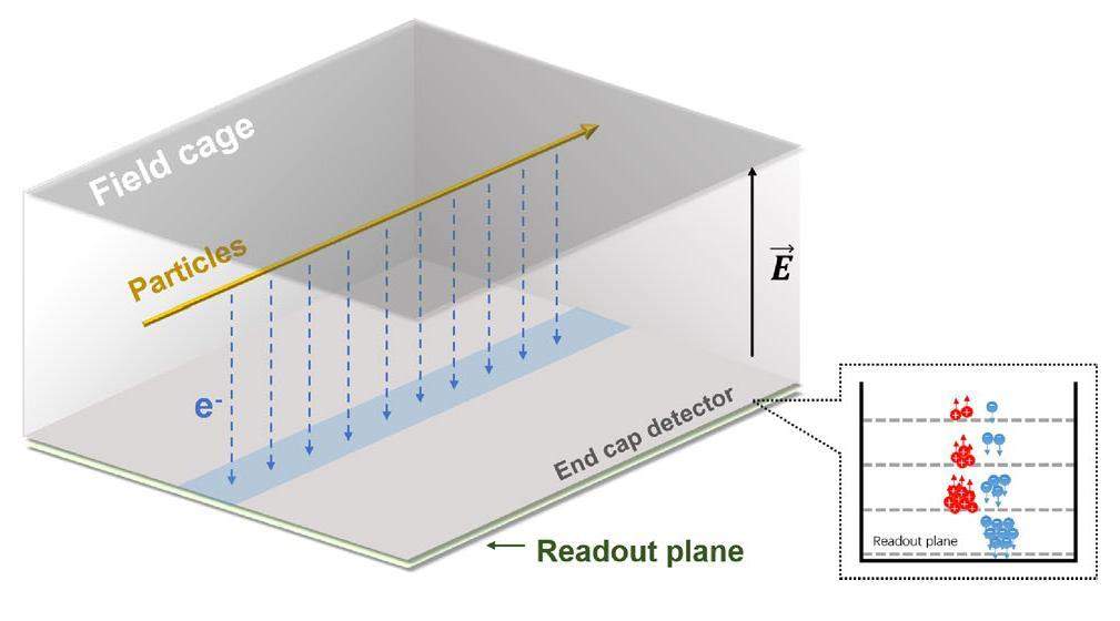
The Time Projection Chamber (TPC), first proposed in the 1970s by researcher David R. Nygren [141] at Lawrence Berkeley Laboratory in the United States, is electronically readable gaseous detector that can directly provide high-resolution three-dimensional track information: x, y, and z coordinates are measured simultaneously along the track. The TPC, filled with gas, mainly comprises three parts: the field cage, the end cap detector, and the readout plane, as depicted in Fig. 31. The field cage consists of a series of electrodes, each connected to a separation resistance of a specific gradient potential, which creates a uniform and stable electric field (E) in its internal region and parallel to the magnetic field (B). When incident particles enter the cage, they ionize the gas medium within the TPC, generating an electron-ion pair. These original electrons drift uniformly toward the end cap detector. The end cap detector is mainly used for the multiplication of electrons. The electrons drift toward the signal readout plane after an avalanche at the end cap detector, which consists of a pad or strip. The fired position on the readout plane records the position of the particles in x and y coordinates. Measuring the drift time t of the electrons with electrons moving at constant velocity v (defined by electric field E of field cage) gives the position of the particle in z coordinate. In addition, the ionization density along the particle trajectory depends on the momentum and the type of the particle. The ionization energy loss (dE/dx), measured by the signal amplititude on each pad or strip, contributes to Particle identification (PID). By arranging the magnetic (B) and electric (E) fields in parallel within the drift volume, the curvature of the trajectory of a charged particle in a known magnetic field can be used to measure the momentum of the particle. Thus, the maximum magnetic field strength is obtained to the extent technically feasible and the gas pressure is kept at a feasible level, resulting in improved resolution by significantly reducing diffusion problems.
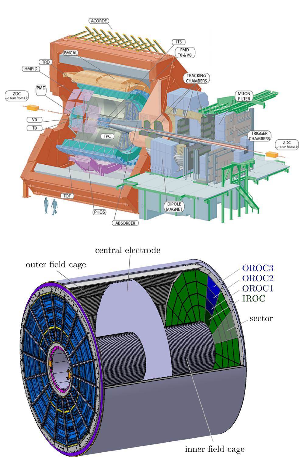
Initially, TPC primarily employed MWPC [142] as the end cap detector. The structure and equipotential lines of the MWPC are illustrated in Fig. 32. This wire chamber [143, 144] consists of two flat cathodes with anode metal wires equidistantly arranged in the middle plane, filled with mixed gas and operating in the proportional zone. The anode wire with positive voltage creates a strong electric field in its vicinity, where electron avalanche amplification only occurs near the wire, inducing a signal (one-dimensional position information of the incident particle) on the anode readout pad close to the filament. Traditional readout structures based on MWPC and pad, such as ALEPH TPC, DELPHI TPC, STAR TPC, and ALICE TPC, have been widely adopted. However, using MWPC as an end cap readout detector has some inevitable drawbacks.
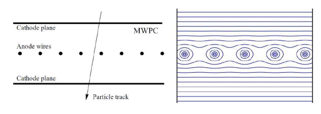
Firstly, the directional nature of the anode wire affects the position resolution and the angle between the track and the wire, resulting in non-isotropic behavior. In addition, the electric and magnetic fields are no longer parallel around the wire, causing electrons to spread in the direction of E × B. It leads to a degradation of position resolution by approximately 600 μm. Furthermore, a positive ion feedback effect occurs, where ions generated by the avalanche cannot be immediate absorbed by the cathode in the drift region, leading to uneven distribution of the drift field. A gate plane is added above the cathode plane to mitigate ion feedback, albeit with a limited count rate. Moreover, due to process technology limitations, achieving wire spacing of less than 1 mm in MWPC is challenging, restricting the position fraction of MWPC to the order of millimeters. Finding new high-performance detectors capable of replacing MWPC is imperative.
With the increasing maturity of printed circuit board technology and microelectronic photoetching technology, Micro pattern structure gas detector (MPGD) [146], e.g., Micromegas and GEM have overcome the early-stage shortcomings of low gain and small sensitive areas while retaining the advantages of high counting rate and high position resolution. As a result, many experiments and studies have optimized and applied these detectors [147, 148].
Micromegas [149, 150] were developed by the French physicist Giomataris Yannis in 1996. The detector is a gas parallel plate detector with a narrow amplification space rely on a new thin metallic micromesh electrode design, as depicted in the Fig. 33. The micromesh structure divides the detector into a drift region of about 3 mm and an avalanche amplification region of only 100 μm. This asymmetrical design achieves a high electric (∼100 kV/cm) in the avalanche amplification region and a low electric field (∼1 kV/cm) in the drift region. As the incident particles pass through the Micromegas detector, energy will be deposited in the drift region and ionized electrons will be released. The resulting electron beam is finally collected by the anode plane of the split strip or pad at the end of the amplification region. Meanwhile, most positive ions drift to the wire mesh and are collected, while the electrons move towards the anode in a narrow funnel due to the high amplification region compared to the drift region. Significantly reducing diffusion and eliminating positive ions. Micromegas offers several benefits, including a high position resolution of ∼20 μm, a high-count rate of up to 108 mm-2s-1 due to its short response time, and a high gain ranging from 104 – 106. Furthermore, it boasts a large detection area, stability in operation, good reliability and uniformity.

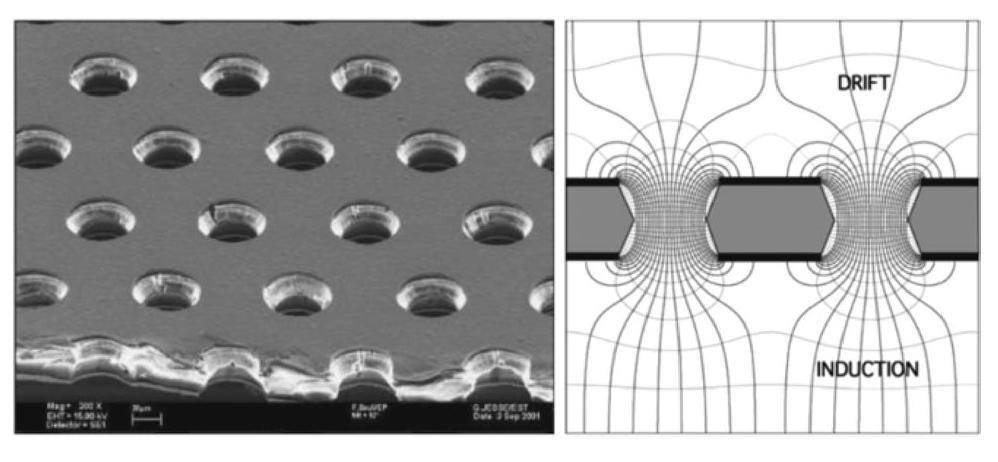
Fabio Sauli from CERN proposed the concept of the GEM [152] detector, which is manufactured by chemically etching small holes, with a diameter of 50–100 μm at high density, on a thin polymer foil coated with metal (e.g., copper). Figure 34 illustrates an electron microscope image of a typical GEM electrode cross-section and an electric field map of the electrode pore area. By applying a voltage of several hundred volts to the metal coating, a strong electric field can be generated within the hole. The electrons released in the upper region drift towards the pore and gain sufficient energy to ionize and collide with the gas molecules. Most of the electrons generated by the avalanche exit the multiplication zone and move to the lower part of the structure, where they can be collected by the electrodes or injected into a second multiplication zone. Compared to wire chambers, GEM technology offers several advantages. It is easier to support, eliminates wire drooping and instability, and can be positioned close to the readout pads, reducing diffusion after amplification. The high-density environment of high-altitude caves ensures uniform amplification over a large area. Additionally, the positive ions generated in the avalanche naturally drift away from the amplification area, preventing the accumulation of space charges. Detector stability and inhibition of positive ion feedback, gain multiplication can be obtained by cascading two or three layers on top of each other. As a result, GEMs and Micromegas are getting popular for TPC [153-155].
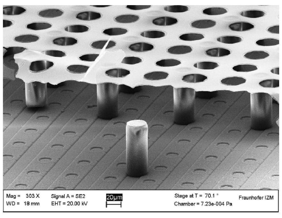
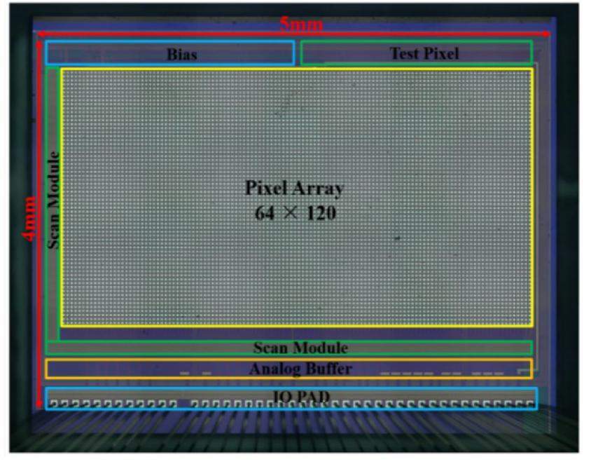
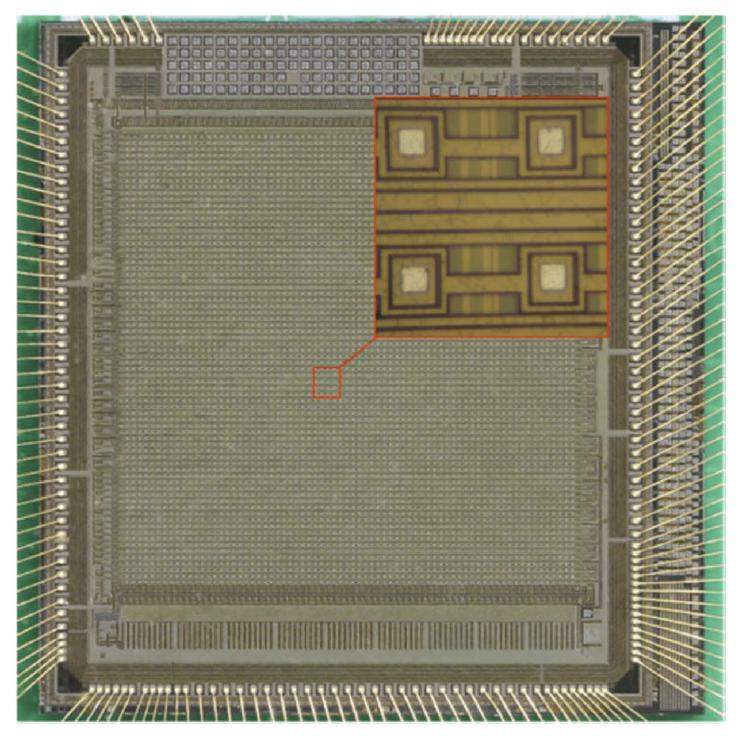
The dimensions of the amplification structure can be reduced from millimeters to about 10 μm by utilizing the micro-structure of the readout anode. However, the pad size of the readout plane does not match the high granularity due to limitations on the integration level of readout electronics. To address this, using silicon pixel sensors with a pixel size of a few microns to read MPGDs is under research. In the first study, combining the Medipix2 chip with a triple GEM stack or Micromegas, a single electron with an efficiency of 90% can be detected [158]. The recent GridPix [159], as shown in Fig. 35 integrates micro-gas amplification and high-density pixelation of ASIC Timepix [160]. With the photolithographic post-processing techniques, GridPix achieves high accuracy in hole position, size, and gap size. As a result, GridPix can effectively detect and separate single primary electrons[161]. The IMPix[81] series pixel sensor, similar to Timepix, can simultaneously measure the charge’s energy, arrival time, and position. Figure 36 is the microscopic photographs of IMPix-S1. The Topmetal series pixel sensor [162, 163] can also collect charge from the sursroundisng media through the exposed part of its topmost metal layer. Figure 37 shows a photo of the Topmetal-II-[164] bonded to a PCB base with gold bonding wire. Both sensors are promising candidates for future TPC applications.
TPC Developments And Frontiers
The first experiment in particle physics using a TPC was the PEP (Fig. 38) experiment at the Stanford Collider in Berkeley Laboratory for the e+ e- PEP-4 collider [165]. The main tracking device in the PEP-4 is a TPC [166] with a drift cavity measuring two times 1 m in length with a diameter of 2 m, as shown in Fig. 39. It consists of a gas-filled sensitive volume, usually with a central cathode that divides the volume into two identical halves. Each side has an anode with a readout system. It is filled with an 80% argon (Ar) and 20% methane (CH4) mixed gas at 8.5 atmospheres and is put in a solenoid magnetic field of 0.32 Tesla. The central membrane of the TPC contains a series of equipotential rings at a voltage of -75 kV, and the position ring at the inner and outer radius of the TPC generates an axially uniform electric field in both parts of the drift chamber. The length of electrons drifting to the two readout planes at each end is 1 meter. As charged particles pass through the cylinder, they ionize the gas along their trajectory, and the resulting ionized electrons drift parallel to the cylinder axis to the end cap sector. Each end cap contains six MWPC sectors for detecting drift ionization, with each sector having 183 anode wires spaced radially by 4 mm. The process of proportional amplification at the wire induces signals on the 2–3 cathode pads nearby [167]. All anode wire and cathode pad signals are sampled through the Charge-Coupled Device at 10 MHz [168] to provide 3-D information (along the drift direction). The Charge-Coupled Device is an analogue shift register capable of storing associated time and pulse-height information [165]. The Charge-Coupled Device record 455 pulse height information and read it at approximately 20 kHz. Thus, for a track traversing the entire radius, there are 15 points of 3D information and 183 (dE/dx) samples for PID. In 1982, this TPC gathered data from the SLAC PEP storage ring and studied 29 GeV e+ e- collisions. When the TPC with the sense-wire spacing 0.4 cm filled with 80% argon (Ar) and 20% methane (CH4) at 8.5 atmospheres pressure, the dE/dx resolution of 6.9% [169] FWHM is reached for isolated tracks, and the tracks in particle jets are measured with a resolution of 8.3% [169] FWHM. It achieves the momentum resolution of about 1.0 p% [165], and the excellent PID was achieved with a resolution of 3.0% [170] for minimum ionizing particles and 2.7% [170] for Bhabha electrons, the excellent value of TPC allowing for the recognition of pions, kaons, and protons in most kinematics.
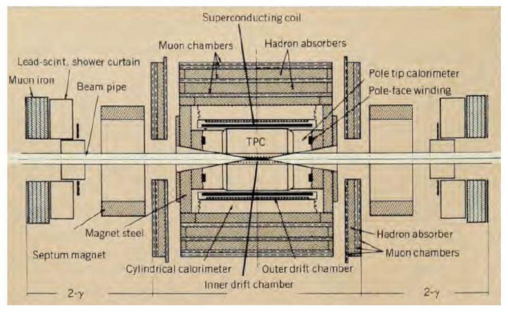
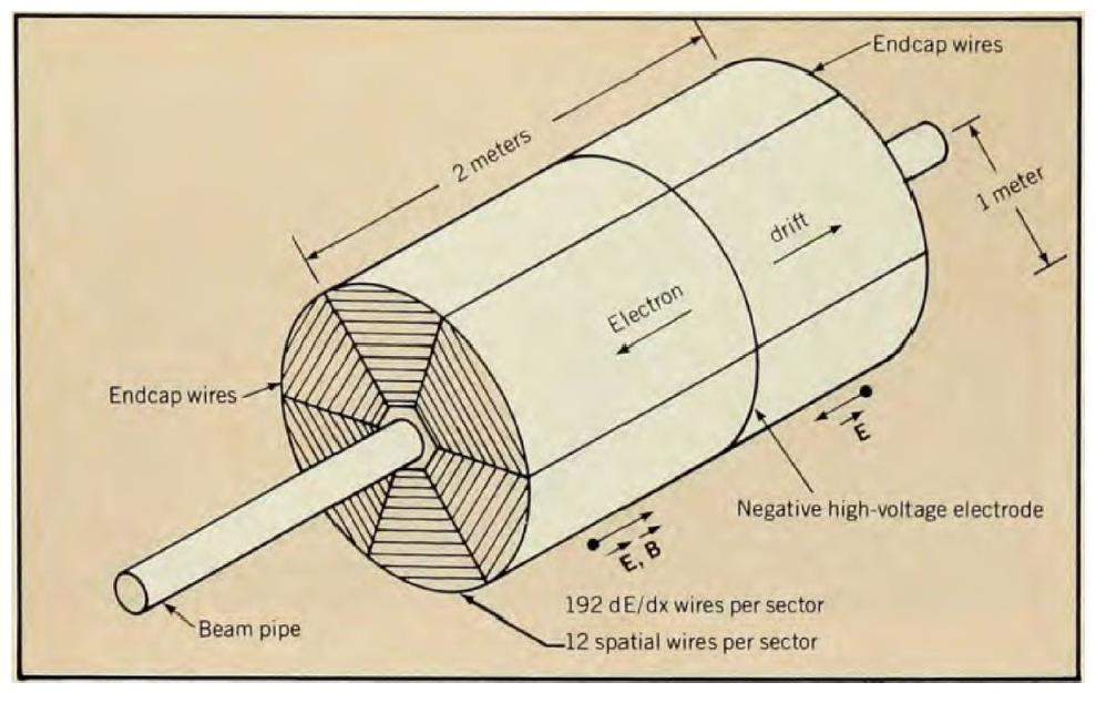
For the same physics, the TOPAZ TPC [171-173] of KEK TRISTAN was proposed in 1986, and the ALEPH TPC [174, 175] and the DELPHI TPC [176] in 1990 and in 1992, respectively, for the LEP at CERN. These TPCs mentioned were used for particle identification and track reconstruction of high-energy particles, capable of handling low event rates with multiplicities of 2–30 charged tracks.
In the early 1980s, as relativistic heavy ion collision research developed, the TPC began to be used in heavy ion experiments, leading to the necessity of addressing higher particle density. The first TPC used to investigate high-energy events in heavy ion physics experiments was the Equation-of-State (EOS) of the Bevalac accelerator Heavy Ion Spectrometer System (HISS) experiment at Lawrence Berkeley Laboratory (LBL) in the United States. The HISS experiment is a target experiment. At the Bevalac, the EOS TPC [177, 178] is greatly expand detector capabilities. It is enable the complete measurement of most charged particles emitted from heavy ion collisions. 3-D tracking will allow the analysis of high multiplicity events with up to 200 charged particles [177]. Accurate tracking resolution in the HISS dipole field and dE/dx information provide momenta and particle identification for the majority of the charged particles of interest. With other components of the HISS system, EOS can observe and identify nearly all charged particles generated in the collisions. LBL designed a 4-channel integrated preamplifier [179] specifically with CMOS technology for EOS TPC. This low-noise, high-dynamic range preamplifier has a switching current source capable of resetting the integral capacitor at the end of each TPC readout cycle. Stuart Kleinfelder also developed a switching capacitor array (SCA) [180, 181] for analog signal sampling and storage for the project. This approach reduces the cost and power consumption of the waveform digitizer, making TPC a practical tool for heavy-ion collision research. Nearly all electronic devices of EOS TPC are located on the detector, a unique design feature that significantly reduces the number of cables leading outside and permits the entire detector to be installed in Bevalac’s HISS magnet. EOS, using full pad coverage, achieved a spatial resolution of 300 μm [170]. When it was filled with P10 gas (10% CH4, 90% Ar) at 1 atmosphere pressure, 128 dE⁄dx samples for PID and the powerful mass separation by dE/dx is demonstrated in [182]. Furthermore, the detector represents an important step towards complete integration and miniaturization of the electronic equipment required by the detector.
Subsequently, Brookhaven’s BNL 810 [183] and CERN’s NA35 [184], NA36, and NA49 [185, 186] experiments all utilized TPC to investigate heavy ion collision experiments. The NA49 advanced the development of these devices by deploying four large TPCs, with the largest pair measuring 3.8 m × 3.8 m × 1.3 m. Two Main TPCs (MTPCL. MTPCR), are situated downstream of the magnets, and two Vertex TPCs (VTPCI. VTPC2), are situated within large dipole magnets [187]. A total of 182,000 SCAs are utilized for readout, which integrates ADCs. At Brookhaven’s RHIC STAR experiment, which operates at higher collision energies of heavy ions, the TPC [188, 189] has a diameter of 4 meters and a length of 4.2 meters. The STAR detector structure is illustrated in Fig. 40. It is filled with P10 gas (10% methane, 90% argon) regulated at 2 mbar above atmospheric pressure [190]. This gas has long been used in TPCs [188]. The STAR TPC achieves a resolution of 350 µm, and an energy loss resolution of 8% for a track that crosses 40 pad-rows with the magnetic field of 0.25 T [188].
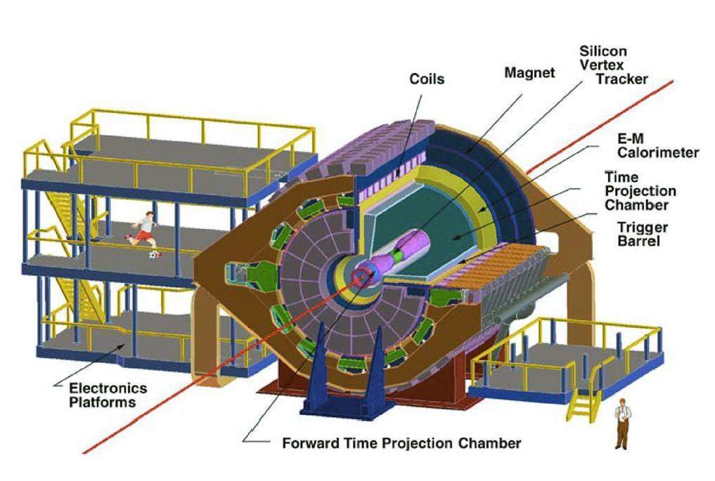
The primary objective of the ALICE experiment at the CERN Large Hadron Collider (LHC) is to investigate Pb-Pb collisions at a center-of-mass energy of 5.5 TeV per nucleon pair. Its TPC [192] aims to handle the exceptionally high charged particle multiplicity resulting from central Pb-Pb collisions at LHC energy levels. It provides charged particle momentum measurement with sufficient momentum resolution, particle identification by dE/dx and by decay topology analysis, and vertex determination in the region pt < 10 GeV/c and pseudorapidities |η| > 0.9. Figure 41 shows a cut-away view of the ALICE detector and a schematic of ALICE TPC. The ALICE TPC, largest of its kind, is a 90m3 cylinder filled with a 90% Ne - 10% CO2 - 5% N2 gas mixture, suited in a 0.5 Tesla solenoid magnetic field. It is divided into two drift zones by the central electrode along its axis, with the field cage ensuring a uniform electric field along the z-axis. The readout plates at two ends are based on the MWPC technique with a total of ∼ 557,568 readout pads. Each readout plate is divided into 18 sectors, each housing an internal readout room (IROC) and an external readout room (OROC). The PASA (preamplifier shaper chip) [193] and ALTRO (ALICE TPC readout chip [194, 195] constitute the ALICE front-end electronics for LHC Run1. Each pad connects to the one of the 16 channels in the PASA chip. Each ALTRO consists of 16 × 10 bit ADCs and the digital logic realizing programmable digital baseline subtraction, tail elimination filter, zero suppression, and multi-event buffer. The use of CMOS ASIC in ALICE TPC results in an extremely compact readout electronics with reduced power consumption, enabling a large number of electronic channels to be positioned close to the detector, thus creating a highly compact and cost-effective system. As the main tracking device of ALICE, this TPC provides the dE/dx resolution ranges between 5–8% depending on the track inclination angle and drift distance, the energy loss, and the centrality in p-Pb and Pb-Pb collisions due to the differing detector occupancy [196].
In LHC Run1, the readout electronics suffered from radiation-induced issues. Thus, in the first long shutdown, the TPC replaced its 216 Readout Control Units [199, 200] to handle the increased radiation load and readout speed in Run2. It was the first time that Flash-based FPGA was employed in physics experiments. Then, in the second long shutdown of the LHC, the ALICE upgraded its TPC detector to accommodate the 50 kHz Pb-Pb collisions in Run3. The upgraded TPC employs GEM technology and continuous readout [201, 202]. A new customized mixed-signal front-end chip called SAMPA will process the GEM signals [203, 204]. The SAMPA chip employs 130 nm CMOS technology with a rated voltage of 1.25 V, featuring 32 channels with optional input polarity and five possible combinations of forming time and sensitivity. Each channel includes a charge-sensitive amplifier, a semi-Gaussian shaper, and a 10-bit ADC, followed by a digital signal processor.
Figure 42 shows the structure of the CSR External-target Experiment (CEE) [207], a spectrometer for research on the properties of nuclear matter at high baryon density regions, which will start physics runs in 2025. The CEE spectrometer [208] includes a TPC [209] at the center of a uniform magnetic field created by a large acceptance superconducting dipole to measure the trajectories of the light-charged particles. The sensitive volume of this TPC is 0.9 m (length) × 0.8 m (height) × 1 m (width), filled with the gas mixture of 90% Ar and 10% CO2 at atmospheric pressure. A large-area GEM foil will amplify the signal to replace the traditional anode wires and address space charge issues arising from positively charged ions drifting back into the sensitive volume. The pad size of the readout will designed as about 5 mm × 12 mm. The total number of channels will be about 15000. These readout pads are connected to the SAMPA ASICs, enabling the CEE-TPC to handle data at an event rate of 10 kHz. This CEE TPC is still under development and commission. The prototype readout electronics provide an energy resolution better than 10% with an input charge of 1.4 fC. Preliminary cosmic ray measurements on the engineering prototype of this TPC with readout electronics show a position resolution of approximately 462 μm (σxz = 461.6 μm) [210].
Small-sized TPCs have a broad range of applications in diverse nuclear physics experiments [211]. The ACtive TARget and Time Projection Chamber (ACTAR TPC) [212-214] at GANIL aim to study the excitation functions with very exotic nuclei, to perform spectroscopic studies beyond the drip line, and the excitation of very collective states such as giant resonances or cluster states. Figure 43 shows the structure of The ACTAR TPC. The active volume is 295 mm × 295 mm × 255 mm encased by a two-wire drift cage connected to the cathode powered via a 20 kV HV feedthrough. The drift cage comprises 20 µm diameter wires with 1 mm spacing in the inner planes and 2 mm spacing in the outer planes, connected by 4.7 MΩ resistors. In the presence of a drifting electric field, ionized electrons generated in the active zone drift toward the pad plane, which is highly segmented into 128 × 128 square pads, each with a side length of 2 mm. The resulting high density of channels (25 channels per square centimeter, for a total of 16,384 pads) was a major challenge in designing the mechanical and pad connections, as well as ensuring that the mechanical deformation of the flange was minimized when applying differential pressures of up to 1 bar. The TPC was successfully produced two gain regions with an incident beam intensity of 20 kHz while kept the capablily of charge measurement. The 1H(18O, 18O)1H and 1H(18O, 15N)4He channels were open and could be distinguished with the scattered heavy-ion identified as being in its ground state [213]. The excitation functions in both channels were reconstructed and fit to obtain the center-of-mass energy resolutions. Resolutions of 38(4) keV FWHM for the (p, p) channel and 54(9) keV FWHM for the (p, α) channel were achieved [213].
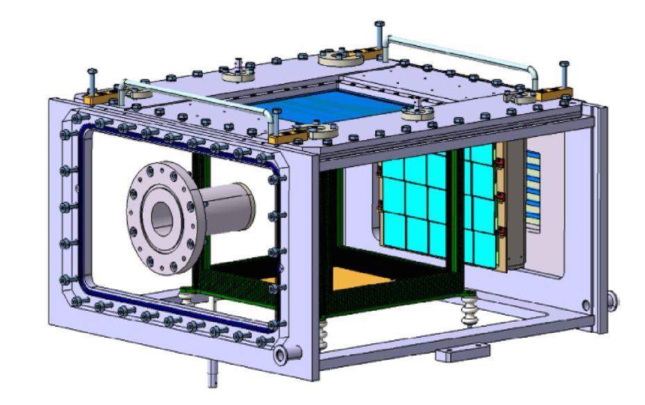
The ACTAR TPC utilizes the General Electronics for TPCs (GET) as a data acquisition system [217, 218]. Figure 44 shows a GET system with a single Micro TCA chassis, which mainly consists of the front-end AsAd (ASIC and ADC) board [216] and the back-end CoBo (concentration board) board. Each AsAd board contains 4 AGET chips consisting of an FPGA (ACTEL ProASIC3E model A3PE1500) and a 12-bit 4-channel ADC. Each AGET chip has 64 input signal channels and 4 fixed-pattern noise (FPN) channels [218]. The AsAd board processes the detector output signals with the AGET [215]. Then, it digitizes the sampled values stored in the analog memory of the AGET SCA with the ADC with a sampling clock of 25 MHz synchronized to the SCA [215, 216]. The longest processing time for reading out the 68 AGET channels is 1.44 ms [216]. The CoBo is a Micro TCA-compatible module (custom PCB and firmware package) developed for the GET system using the Xilinx Virtex-5 System-on-Chip, which contains an FPGA and dual PowerPC440 CPU cores. The CoBo board receives the digital data from the AsAd through the VHDCI connections at a maximum data rate of approximately 1.2 Gb/s [215], processes it, and transfers it to the storage field. Each Cobo can handle up to 4 AsAds boards with 1024 detector signal channels [216]. The MUTANT module (MUltiplicity ANd Trigger) synchronizes the boards and handles the triggers and timestamps. Given the generic approach, the system has been used in many nuclear, particle, subsurface, and medical physics applications.
Plenty of small-scale TPCs have been built across the world. The TexAT (Texas Active Target) detector [220-222] was constructed at the Cyclotron Institute Texas AM University for nuclear structure and astrophysics experiments with rare isotope beams [219]. Figure 45 shows the structure of the TexAT. It is designed for general use in nuclear structure and astrophysics experiments with rare isotope beams. It combines a highly segmented TPC with a two-layer solid-state detector, offering high accuracy and flexibility for experiments with low-intensity exotic beams and enabling 3D trajectory reconstruction of incoming and outgoing particles involved in nuclear reactions and decay. The MATE (Multipurpose time projection chamber for nuclear AsTrophysical and Exotic beam experiments) at HIRFL studies the reactions at stellar energies [223, 224]. Figure 46 hows the schematic diagram of the MATE-TPC with a gating grid. MATE possesses an active volume of 300 mm × 300 mm × 200 mm [224] in the form of a triple-wire field cage and a pair of thick GEMs mounted on top of the readout plate with 4000 channels. The versatile multipurpose time projection chamber (MTPC), with a cylindrical sensitive volume with a 140 mm diameter, has been proposed at Back-n [225], designed primarily for light-charged particle emission reactions but also adaptable for other measurement types such as fission reactions, neutron beam profiling, neutron imaging, etc. The 1519 [225] signal channels are read out with micromegas connected to a scalable readout system. The GET system reads the signals in TexAT and the MATE, and the MTPC readout system is developed with AGET ASIC.
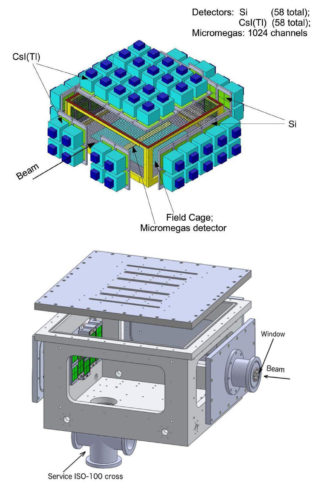
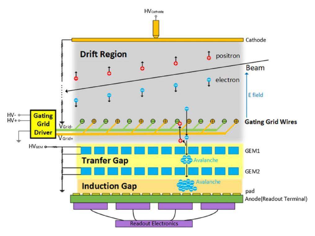
In recent years, TPC has been introduced for studying rare physics, especially in searching dark matter and neutrino-less double beta decay (0νββ), due to the good performance in tracking capabilities, stability, radiopurity and scalability.
Weakly interacting massive particles (WIMPs) remain one of the most promising directions for dark matter research. Dual-phase (liquid and gas) TPCs are popular for dark matter search by detect the WIMP [227]. Figure 47 shows the principle of the dual-phase TPC. When a dark matter particle interacts with liquid argon or xeno [228, 229], it generates two signals: one from the prompt scintillation (S1) and the other one from ionized electrons (e-). The electrons drifted into gas, creating a delayed secondary light signal (S2) by proportional scintillation. The S1 and S2 are detected by photomultiplier tubes (PMTs) installed at the top and bottom of the TPC. Combining the S2 signal observed on the top PMT and the time interval between the S1 and S2 reconstructs the three-dimensional coordinates of the interaction position. Background events are rejected by the ratio between S2 and S1 and the number of S2 signals. The XENON [230] is a project for direct dark matter search at the Laboratori Nazionali del Gran Sasso (LNGS). The XENONnT is shown in Fig. 48, the latest member in this project, has a cylindrical TPC, 148 cm long and 137 cm diameter, filled with 5.9 tons of liquid xenon. With an exposure of 20 ton × year, XENONnT is expected to reach the highest sensitivity of 1.4 × 10-48 cm2 for a WIMP of 50 GeV/c2 [231], which is an order of magnitude below the limits set by the XENON1T [232].
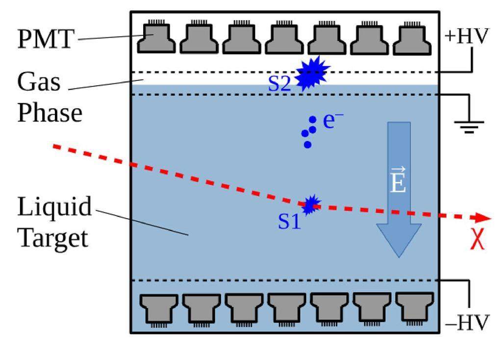
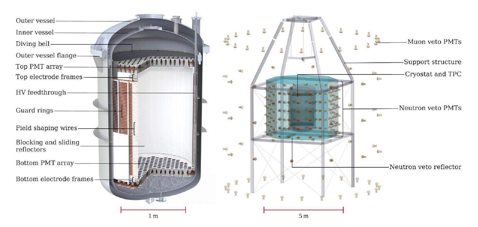
The PandaX-4T experiment [233], located at China Jinping Underguoun Laboratory (CJPL) [234, 235], is the first multi-tonne liquid xenon detector operating in the world. Its large cylindrical TPC which is shown in Fig. 49, with a transverse diameter of 1.2 m and a height of 1.3 m, holds 3.7 tons of liquid xenon. It has 169 and 199 photo-multipliers (PMTs) on the top and bottom of the TPC, respectively. The data from PandX-4T set a stringent limit to the dark matter-nucleon spin-independent interactions, with the lowest excluded cross-section (90% CL) of 3.8 × 10-47 cm2 a WIMP of 40 GeV/c2 [236].
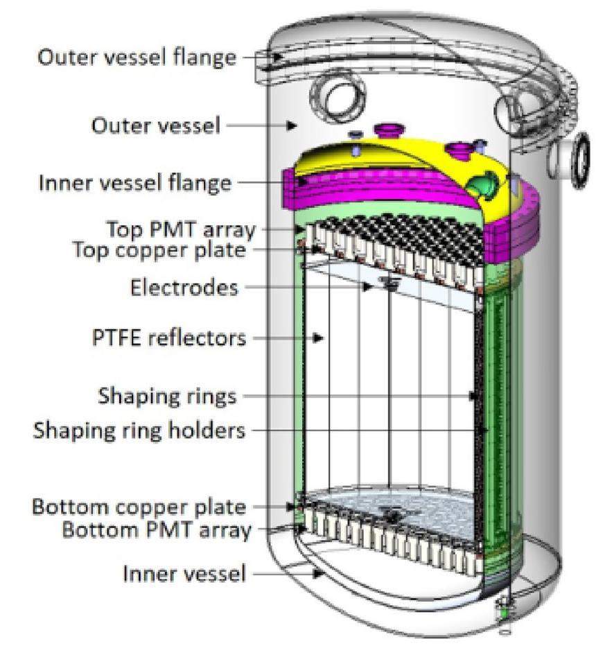
There have been several experiments aimed at searching for 0νββ in a number of different candidate isotopes [238] such as 136Xe and 82Se, which has also been suggested as a promising isotope in the search for 0νββ. The PandaX-III employ high-pressure Xe TPC and EXO-200 employ liquid Xe TPC looking for 0νββ in the 136Xe. The NνDEx experiment utilizes a high-pressure Se TPC searching 0νββ in the 82Se. The prototype experiment of the Enriched Xenon Observatory (EXO) EXO-200 currently operating at WIPP (Waste Isolation Pilot Plant) and using a TPC in a cylinder shape with 40 cm diameter and 44 cm length and contains ∼ 175 kg liquid Xe enriched to 80.6%[239]. Cutaway view of the EXO-200 setup as shown in Fig. 50. The TPC is held in a low-background cryostat system filled with high-purity HFE7000 fluid to keep the temperature of liquid xenon at 167 K and shield the radiation. To improve energy resolution, this TPC simultaneously records the ionization and scintillation signals in the liquid. The TPC cylinder contains two identical drifting sectors formed by a biased cathode grid in the middle. The end of each sector consists of two wire grids crossed at 60∘ and an Large-area avalanche photodiodes (LAAPD) array. The incident particle ionizes the xenon atoms and generate electrons. The ionized electrons drift towards the wire grid, providing two-dimensional localization. Some xenon ions recombine with the electrons before they drift away, inducing excited states in the xenon atoms. Upon relaxation of the excited atoms, they emit ultraviolet light, referred to as scintillation, which the LAAPD captures. The time interval between the light and ionization signals reconstructs the (longitudinal) coordinate. In addition, combining the light and the ionization signal also provides better energy measurement. In August 2011, the EXO-200 first observed double beta decay in 136Xe [240]. In 2014, the EXO-200 experiment set a lower limit on the 0νββ half-life in 136Xe at 1.1×1025 years at 90% CL [241]. The next-generation Enriched Xenon Observatory (nEXO), with 5000 kg of isotopically enriched liquid xenon, is expected to reach a half-life sensitivity of 1.35×1028 yr at 90% confidence level in 10 years of data taking [242].
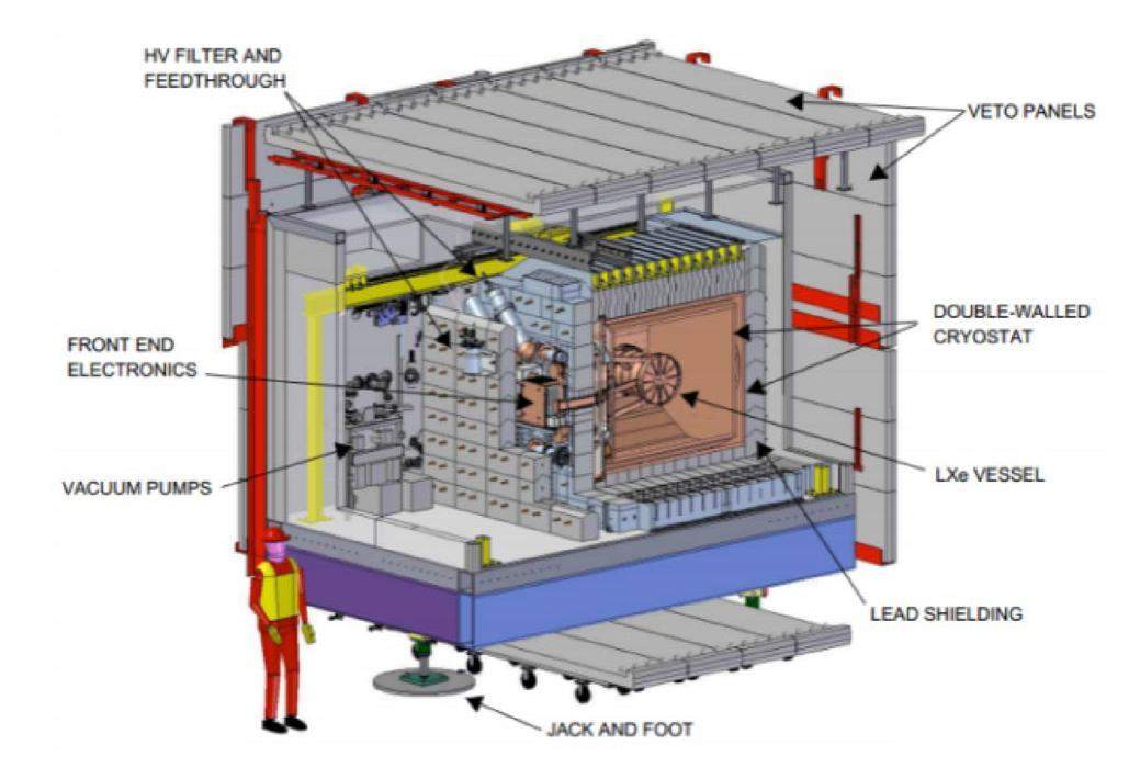
The PandaX-III [244] (particle and astrophysical xenon experiment III) experiment uses gas TPC to search 0νββ in 136Xe at the China Jin-Ping underground Laboratory II (CJPL-II). The schematic of the PandaX-III TPC is shown in Fig. 51. The gas TPC can reconstruct the 3D trajectory and the energy deposition for every single track, which significantly improves the background suppression. The first phase of PandaX-III uses a cylindrical TPC of 1.5 m in diameter and 2 m in length, filled with 140kg of 99% 136Xe and 1% TMA (trimethylamine) at 10 bar [245]. Tine pitch micro-pattern gas detector (Microbulk Micromegas), employed at both ends of the TPC, incorporating a cathode in the middle, accomplishes the readout of the drift charge. The 140kg level PandaX-III experiment expects to achieve an energy resolution of 3% FWHM, a signal efficiency of 35%, reaching a half-life sensitivity of 0νββ (90% CL) of 8.5 × 1025 years after three years of operation [245]. The second phase of the PandaX-III, in ton-scale, will consist of five TPCs in the same water tank, with improved energy resolution and background shielding [246].
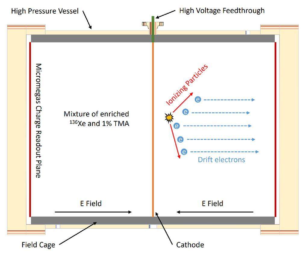
As depicted in Figure 52, the NνDEx[247] (No neutrino double-beta-decay Experiment) uses high-pressure gas TPC with silicon pixel sensors-based readout to search 0νββ in 82Se. If double beta decay happens in 82Se, two emitted electrons ionize the gas, creating sinuous trails with a Bragg peak at each end. In 0νββ, the total energy of the two electrons is 2.996 MeV. Due to the electronegativity of Se, the rapid formation of negative ions between electrons and surrounding Se molecules makes avalanche amplification impossible, it is necessitating very low noise in the readout plane. The charge readout plane consists of a self-developed Topmetal [248] pixel sensor that directly collects and reads the initial ionized charge without amplification. This approach circumvents the fluctuations introduced by the traditional TPC avalanche amplification process. The specific design of the electric field structure achieves 100% charge collection efficiency. Hence, the NνDEx aims to reach 1% energy resolution near the Q value of 2.996 MeV. The time interval between different ions determines the drift distance. The NνDEx experiment can reconstruct each event’s trajectory and ionization deposition. The NνDEx-100, which is being built with 100 kg of SeF6 gas, is scheduled to be installed at CJPL around the year 2025. In the future, the NνDEx will be scaled to a ton-scale.
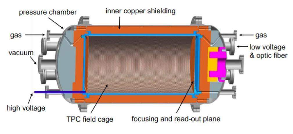
The rapid advancement of TPC has extended its significance to space exploration. The Low-Energy X-ray Polarization Detector (LPD) [249] is one of the payloads in the POLAR-2 experiment, designed as an external payload for the China Space Station (CSS) deployment in early 2024. Figure 53 illustrates the mechanical structure of the LPD. The LPD utilizes a charge-TPC structure with pixel sensors as its readout to observe the polarization of Gamma-Ray Bursts (GRBs) prompt emission in the energy range of 2-10 keV, with a wide field of view (FoV) of 90 degrees. The detector comprises 81 units, including a cathode, a gas microchannel plate (GMCP), a pixel readout chip (Topmetal-L), and a gas-sealed chamber.
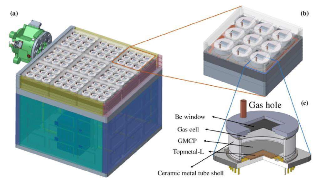
The Electron-Tracking Compton Camera (ETCC) reconstructs the three-dimensional tracks of the scattered electron in the Compton process for both sub-MeV and MeV gamma rays. Figure 54 illustrates diagram of the ETCC. The ETCC typically comprises the gaseous electron tracker and the surrounding position-sensitive scintillators. Gamma-ray incident to the ETCC makes a Compton scattering in the gaseous electron tracker, which detects the scattering direction and energy of the Compton-recoil electron. The scintillators detect the absorption point and energy of the Compton-scattered gamma ray. The ETCC has been installed on the Sub-MeV gamma-ray Imaging Loaded-on-balloon Experiment (SMILE) series [250]. The ETCC on the SIMLE series uses a TPC with a micro-pixel chamber (μ-PIC) as the gas electron tracker. In the SMILE-2+ balloon, the 30 cm3 cubic TPC fills with the gas ratio of Ar: CFA: iso-C4H10=95 : 3 : 2, and the position-sensitive detector is made of GSO scintillators.
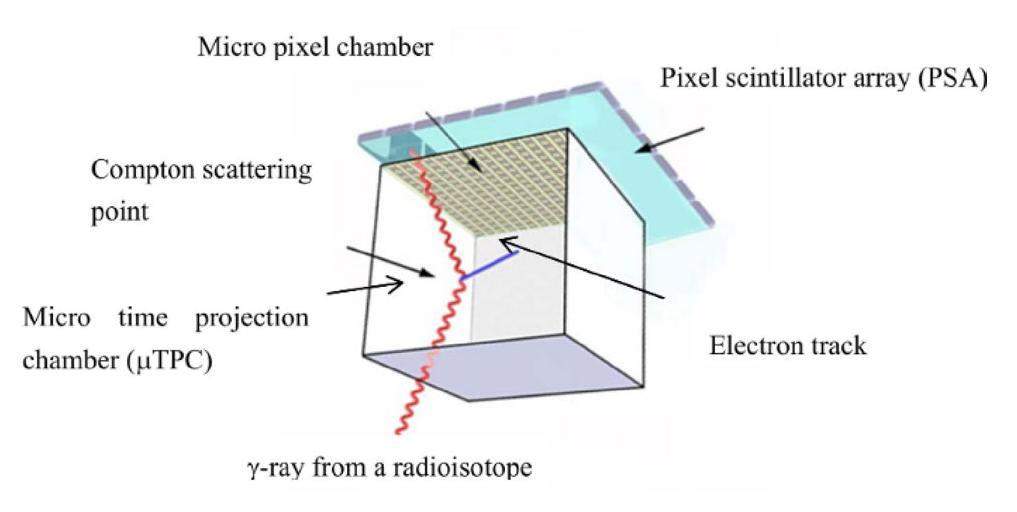
The silicon pixel sensor has shown great potential in real time beam monitoring. The researchers from IMP proposed the Hi’Beam detection systems [252-255] based on silicon pixel sensors designed to fulfill the beam monitoring requirements at the HIRFL and HIAF. Figure 55 illustrates the general principle of the Hi’Beam-SEE, which is composed of two detector systems with silicon pixel sensors acting as the anode. When charged particles pass through the detector field, they ionize the gas and produce electron-ion pairs. The anode then captures the charge in the presence of an electric field to reconstruct the trajectory of the particles. Two detector systems are positioned perpendicular to each other to reconstruct the 3-D profile of the beam. The HiBeam series includes the HiBeam-A [252, 253] for accelerators, the HiBeam-T [254] or physics terminals, and the HiBeam-SEE [256] for precise single event effects locating. The HiBeam-A prototype employs a microchannel plate (MCP) to amplify the rare ionized charge in the high vacuum chamber and one pixel sensor to collect the charge, demonstrating a spatial resolution of ∼ 5 μm. The HiBeam-T prototype features a gas chamber with P10 gas (composed of 90% Ar and 10% CH4) and utilizes a gating grid to prevent the pixel sensors from becoming saturated with a high particle rate. The preliminary test results shows a resolution ∼ 30 μm [254]. The HiBeam-SEE reconstructs the trajectory of individual particles in the beam to infer their point of impact on the device under test. It uses air directly as the gas, primarily capturing the charge from the oxygen ion that combines the ionized charge. The first test with its prototype indicate a spatial resolusion better than 2 μm for Ta particle [255]. The HiBeam-A and HiBeam-T prototypes use the Topmetal-II sensor, while the HiBeam-SEE uses Topmetal-M. In the near future, the IMPix-S sensor will be integrated into the HiBeam system. With a similar principle as Hi’Beam, the HIRLF-CSR CEE experiments are building a silicon pixel sensor-based beam monitor, providing a spatial resolution better than 50 µm and a timing resolution better than 1 μs [257]. The first prototype of this beam monitor uses the readout based on the Topmetal-II- chip [258]. The second prototype is using the Topmetal-CEE pixel sensor for the readout [259].
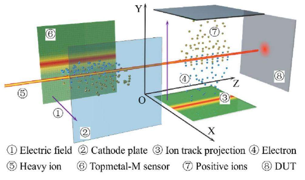
The Time Projection Chamber (TPC) was initially employed as a tracking detector. It has since found widespread use in various particle physics experiments. As new scientific challenges emerge and technology and science continue to advance, the TPC has been continuously developed to enhance its capabilities in terms of high resolution, high count rate, and low noise. Consequently, it has found increasingly extensive applications in nuclear physics experiments, rare physics phenomena experiments, space detectors, etc.
Multigap Resistive Plate Chamber Detector
Introduction
To reveal the physics in the high energy particle collisions, it is important for spectrometers to reconstruct and identify the secondary particles (i.e. Particle Identification, PID)[264]. Figure 56 shows the π/K separation powers of TOF systems given a fixed flight distance of 8 meters, where σTOF is the time resolution of the TOF system. Simply distancing the detectors is not practical since the coverage area and the cost rise quadratically. Thus, high time precision is crucial to recognize high momentum particles.
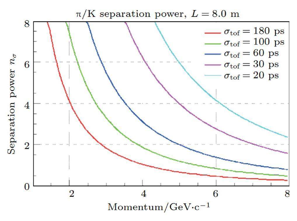
However, timing performance is not the only consideration for building a TOF system. Due to the momentum measurement by the tracking detector, the spectrometer must be operated in high magnetic field, so the material and signal propagation of the TOF detectors must not be affected, especially for the detectors installed within the magnet. Moreover, the total active areas of the TOF detectors, in order to cover the phase space at several meters’ distance, are usually in tens of m2, even over 100 m2, making the cost of the detectors nonnegligible [266].
Since the 1990s when the novel structure Multigap Resistive Plate Chamber [267] (MRPC) was invented, it has been widely applied to many high energy physics experiments, such as BESIII [268], ALICE [268, 269], CBM [270], STAR [270, 271], and MPD [272]. Compared with other technologies such as fast scintillator with photomultipliers (PMT or SiPM), the competitive edge of the MRPC has been verified: the theoretic intrinsic time resolution is about 10 ps [273], and the best reported resolution is as low as 16 ps [274]; in large experiments MRPCs works stably with time precisions in 60 ps level and show good tolerance in magnetic fields; the components of the MRPCs are in low prices and can be easily produced in large area. Table 1 lists the representative high energy physics experiments around the world which apply MRPCs for time measurements.
| ALICE | STAR | FOPI[275] | HADES[276] | BESIII | CBM | SoLID[277] | BM@N[278] | MPD | |
|---|---|---|---|---|---|---|---|---|---|
| Active area per detector (cm) | 120 × 13 | 22 × 8.4 | 90 × 4.6 | 60 × 2 | 0.5 × (9.2 + 14.8) × 32.8 | 33 × 27.6 | – | 35.1 × 16 | 64 × 30 |
| Total active area (m2) | 141 | 50 | 5 | 8 | 1.33 | 120 | 10 | 12 | 52 |
| Pad size (cm) | 3.7 × 2.5 | 6.3 × 3.1 | 90 × 0.3 | 60 × 2 | (9.1 ∼ 14.1) × 2.4 | 27 × 1.0 | (16 ∼ 28) × 2.5 | (16 ∼ 56) × 1 | 64 × 1 |
| Gap × thickness (mm) | 10 × 0.25 | 6 × 0.22 | 8 × 0.22 | 4 × 0.3 | 12 × 0.22 | 10 × 0.25 | 10 × 0.25 | 10 × 0.3 | 15 × 0.2 |
| Gas mixtures (C2H2F4/iC4H10/SF6) | 90/5/5 | 95/5/0 | 85/5/10 | 98.5/1/0.5 | 90/5/5 | 90/5/5 | 90/5/5 | 90/5/5 | 90/5/5 |
| Operating field (kV/cm) | 96 | 107 | 110 | 107 | 109 | 110 | 106 | 114 | 120 |
| Efficiency | 99.9% | 95 - 97% | 97 ± 3% | > 95% | 99% | 97% | 98% | 95% | 98% |
| Time resolution (ps) | 40 | 60 | 73 ± 5 | 70 | 60 | 60 | 20 | 65 | 40 |
| Max rate (Hz/cm2) (kV/cm) | 50 | 10 | 50 | 700 | 50 | 30k | 10k | 5k | 2k |
Working Principle And Performance Of MRPC
MRPC is a gaseous detector with resistive plate electrodes and multigap structure. The common working gas for MRPCs is a mixture of Freon, iC4H10 and SF6 with a fraction of 90/5/5. High electric field is applied between the gas gaps so that the primary ionization by an incident particle will immediately start a Townsend avalanche[279] which has an exponential grow-up of charge and a quench by the electronegative gas and space-charge effect. The usage of the resistive electrodes is to limit the voltage drop to a local area (mm2 magnitude), ensuring the sensitivity for another region. The multigap structure results in the ordered gas gaps of hundred-micron level thickness. The narrow gap limits the avalanche spatially and allows MRPCs to be operated in even higher fields, e.g., above 105 V/cm. As a result, the electron drift velocity vd and effective Townsend coefficient α* increases and the time resolution is improved significantly. The intrinsic time resolution of the MRPC is estimated by the following equation[280]:
Figure 57 shows the structure of the MRPC. Usually, nylon fish lines with specific width are used to sustain the gas gaps. Carbon layers with surface resistivity in MΩ/
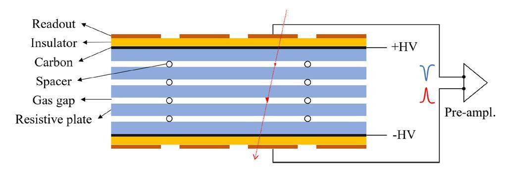
When the electron-ion pairs are avalanched and drifted in the gas gaps, they will induce a current signal on to the readout electrodes which are usually laid on a PCB in shape of strips or pads. For the case of corresponding readout strips in Fig. 57, differential signals are transmitted to the electronics on both ends. If the readout strips are long with nonnegligible signal propagation time, both-end readout is essential for reconstructing both the hit time and position.
The behavior of current through the resistive electrodes constitutes the basic principle of the ’Ohmic Model’ [281], which is very useful to understand and evaluate the rate capability of an MRPC. The resistivity of the electrodes leads to a voltage drop ΔVel given a current I which is determined by the incident flux Φ. It can be described as the following equation:
Typical Applications Of MRPCs
One of the most successful applications of the first generation MRPCs is that on the STAR-TOF system [283]. A barrel-shape array of MRPC detectors surrounds the central Time Projection Chamber (TPC). The total active area for STAR-TOF reaches about 60 m2, including 3840 MRPCs with 23040 readout channels. The STAR-TOF MRPC has 6 gas gaps of 0.22 mm thickness. The electrodes are made of float glasses of 0.7 mm thickness whose bulk resistivity is in 1012 Ω cm level. Each MRPC contains 6 readout pads of 3.1 × 6.0 cm2. The working gas is the Freon and SF6 mixture in a fraction of 95/5.
The readout chain for STAR-TOF MRPCs is the NINO-based [284] front-end electronics (FEE) and the high-precision time-to-digital converter (HPTDC) [285]. NINO is an ASIC chip developed by the group in CERN for the amplification and discrimination of the differential MRPC signals. To realize the precise timing purpose, the designed LVDS output of discriminated signal has a rise time within 1 ns. The power consumption of NINO is as low as about 45 mW per channel. The overall time jitter of the STAR-TOF readout chain is better than 25 ps. NINO discriminates the time when a signal exceeds or descends to the threshold. The time-over-threshold (TOT) positive correlated to the signal amplitude or charge and is very useful to correct the time-walk caused by the amplitude difference. With time-slewing correction, the time resolution for STAR-TOF MRPCs reached 60 ps during the beam test.
The second generation MRPC, featured of an expanded rate capability over 20 kHz/cm2, is developed for high-rate conditions. The interaction rate of the existing and proposed experiment has been increasing for better statistics and rare physics probe finding. The compressed baryonic matter spectrometer (CBM) [286] is one of these typical experiments for which the designed interaction rate will reach 10 MHz. As a fixed target experiment, CBM measures the products of heavy ion collisions with beam energies up to 11 GeV/u. Thus, even though the TOF wall is placed at 10 m from the target with a total active area of 120 m2, the counting rate for MRPCs at the central region still reaches 30 kHz/cm2, which is a huge challenge for MRPC. As equation (2) indicates, the most effective way to improve the rate capability is developing low resistivity novel materials for the resistive plates. Since 2008, the high energy physics detector group in Tsinghua University has been dedicated to the low-resistive glass. By many efforts of tests and optimizations on the components and techniques, the TUYK-LRG10 low-resistive glass has been successfully developed [284, 285], whose typical features are listed in Table 2. The real-size MRPC prototypes for CBM-TOF have been tested under the high intensity electron beam in Helmholtz-Zentrum Dresden-Rossendorf (HZDR), Germany, showing a capability as high as 70 kHz/cm2 (with efficiency > 90%) and a time resolution better than 80 ps [287].
| Parameter | Value |
|---|---|
| Standard size (mm2) | 330 × 276 |
| Bulk resistivity (Ω⋅cm) | ∼1010 |
| Standard thickness (mm) | 0.7, 1.1 |
| Thickness uniformity (μm) | 20 |
| Surface roughness (nm) | < 10 |
| Dielectric constant (F/m) | 7.5–9.5 |
| Accumulative charge tolerance (C/cm2) | > 1 |
The CBM-TOF wall is divided into three regions according to the rate conditions [288]. The inner region is built with MRPC1a, 1b, 1c, operated under the rate condition between 5–30 kHz/cm2. The MRPC2, developed by Tsinghua, is for the intermediate rate region with condition about 5 kHz/cm2. The MRPC1 series and MRPC2 are assembled with low resistive glass. The MRPC3 and 4 take up the low rate region and are made up of thin float glass. Figure 58 shows the picture of the MRPC2 detector. It consists of double stacks with 8 gas gaps of 0.25 mm thickness, 32 readout strips of 27 × 1 cm2. Each TOF module houses 5 MRPCs with PADI [289], the FEE board, plugged directly on the detectors. Then the discriminated signals are transmitted to the GET4-TDC [290]. 108 MRPC2 detectors were first installed on the endcap of the STAR thanks to the FAIR-Phase0 collaboration [191]. They have played an important role in expanding the phase space η from 1.1 to 1.6 for STAR during the BES-II runs [292].
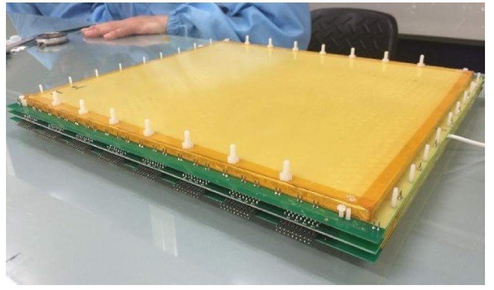
As high rate MRPCs being developed and tested, the gas related effect becomes an important issue for the stable and sustainable operation of the second generation MRPCs. Firstly, Freon and SF6, as main components of the working gas, have serious greenhouse effects. The regulations to the greenhouse gases in EU, China and other countries may lead to uncertain situations on the availability and cost. There have been continuous efforts [288-290] on the substitutes of the MRPC working gas, such as HFO. However, it is also important to decrease the gas consumption especially for large area MRPC-TOF system. Secondly, gas pollution effects characterized by the increase of dark current and noise rate under persistent irradiation were observed at mini-CBM, another phase0 program of CBM dedicated for high rate tests. The gas pollution effect has been studies by means of both the simulation and test, and we find that the main cause is the accumulation of ionized gas pollutants in gas gaps due to the inefficient gas exchange [293]. Without a delicate structure for pressure-driven gas exchange, the resistance of thin gas gaps in traditional MRPCs significantly restrict the gas exchange to a diffusion level. The gas pollutants, if not expelled in time, may result in unexpected noise discharge in gas gaps or even the creepage along the fishline spacer. There have been observations showing the noise patterns and glass microscopic damages at the fishline region, as displayed in Fig. 59 [294].
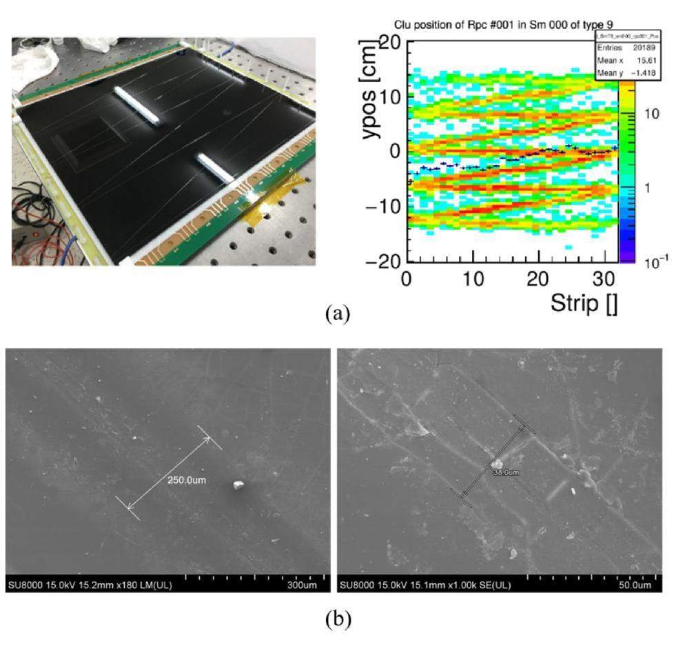
To solve this essential problem, a novel structure called the sealed MRPC has been developed [295]. For each sealing gas chamber, a 3D-printed sealing frame is spiced with the PMMA panels, as shown in Fig. 60(a). The gas tubes and fishline layout are carefully designed so that the gas can be flushed directly through the gas gaps. The sealed MRPC prototype has been tested under cosmic rays and X-rays, showing promising performances: the efficiency reaches 97%; the time resolution is around 60 ps at working point; the operational currents are constant at fixed rate conditions and decays in seconds to a low level after the irradiation.
A prospective candidate of new spacer is the cylindrical mylar pads. The rectangular cross section may have minor distortion to the neighboring electric fields, and the resistivity of mylar is higher than the fishline. Figure 61(b) shows the layout of the mylar spacers pasted on the electrodes, it is estimated that the total contact area of spacers on the glass is a half of that of fishlines, implying that smaller dead zone is achieved at the same time. A first prototype has been tested, showing promising first results, see Fig. 36.
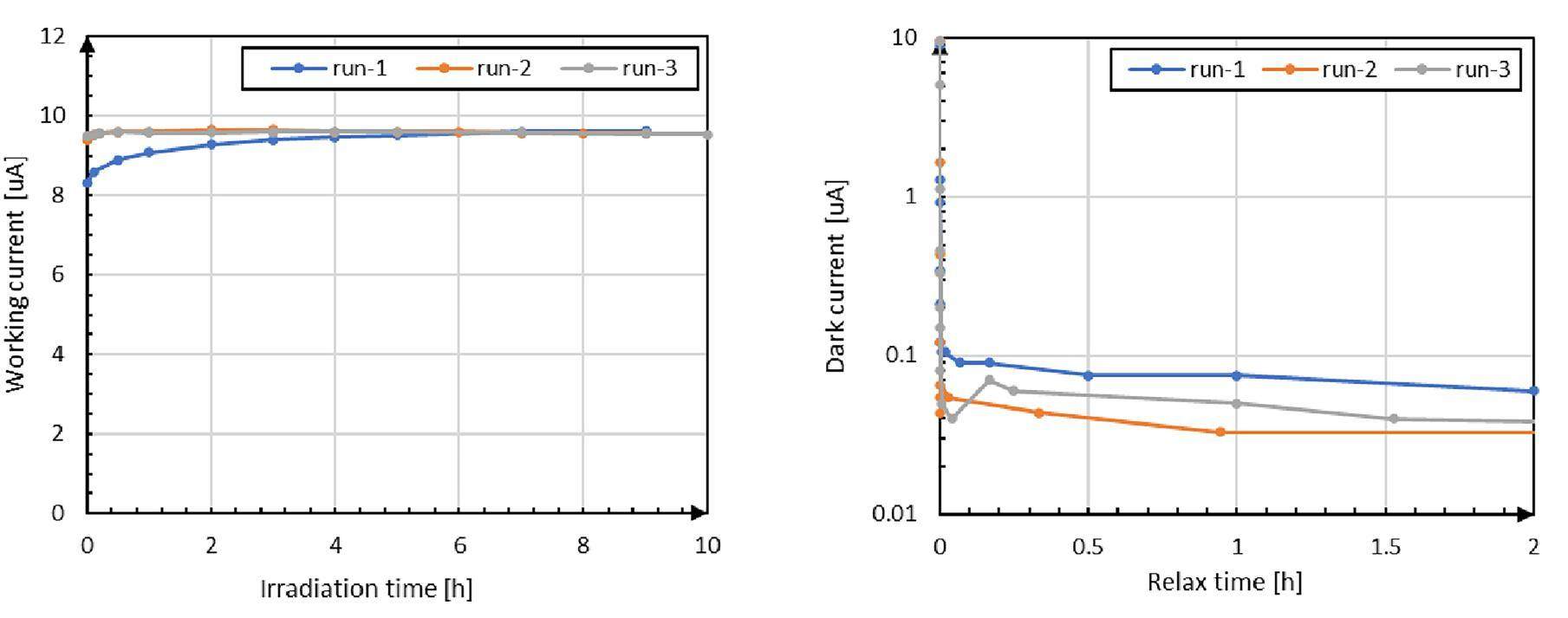
The experiments with low rate conditions can also benefit from the application of the sealed MRPC, since the gas consumption can be saved significantly. The external TOF system (eTOF) [296] of the CSR External-target Experiment (CEE) [208] in Lanzhou, China will be the first application of the sealed MRPC. For eTOF MRPCs, the outermost glass electrodes are glued with the sealing frame instead of the PMMA plate because the float glass is of higher mechanical strength. Performances of the real-size prototypes have been validated in cosmic and beam tests. The efficiency reaches 98% with a time resolution better than 60 ps [297]. It is very exciting to see in Fig. 62 that the prototype works in stable performance with a gas flow as low as 1 sccm, lasting for 21 days. It is estimated that no more than 70 sccm gas flow is needed for the 3.2×1.6 m2 active area of the eTOF wall, which is a reduction to about 1/10 compared with the typical flow rate if using traditional MRPCs.
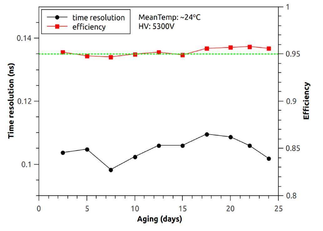
The third generation MRPC is proposed for the future applications when the requirements are drawn to the ultimate limit of the detector physics. A typical example is the proposed SoLID [277] experiment at JLab, which is expected to realize high energy collisions between electrons and target for nucleus structure studies. The TOF system should be able to separate kaons and pions at 7 GeV/c moments, requiring a time resolution in 20 ps level. Besides, the rate condition is estimated as 20 kHz/cm2. To reach a time precision less than 20 ps, both the time jitter of MRPC and the electronics must be less than 14 ps. With narrow gas gaps, MRPC can reach a 10 ps intrinsic resolution according to the simulation. However, time jitter of the NINO (PADIX) + HPTDC (GET4) used in the first and second generation TOF spectrometers is generally greater than 20 ps. Thus, a new generation technology of fast Switched Capacitor Array (SCA) chip based waveform sampling is proposed with typical bandwidth of 650 MHz and sampling rate over 5 GHz [298]. Diagram of this high resolution technology is shown in Fig. 63. With details of signal waveforms available, more information can be excavated for the reconstruction of time. For example, a study [274] has successfully outperformed the traditional time-slewing correction using the deep learning models, as shown in Fig. 64. It trained a model called ComLSTM using the simulated MRPC signals for the recognition of start time of the avalanche, and tested the model performance with test data. Structure of this model can be seen in Fig. 65. The simulation was carried out by a standalone MRPC simulation framework based on GEANT4. Two identical MRPC prototypes and the relevant electronics have been designed and produced. The MRPC has 32 gas gaps of 104 um thickness. Accordingly, the working point rises to about 150 kV/cm. Time resolution is analyzed by the ComLSTM model, showing result of 16.8 ps, see Fig. 66. Timing performance has fulfilled the requirements for both methods.
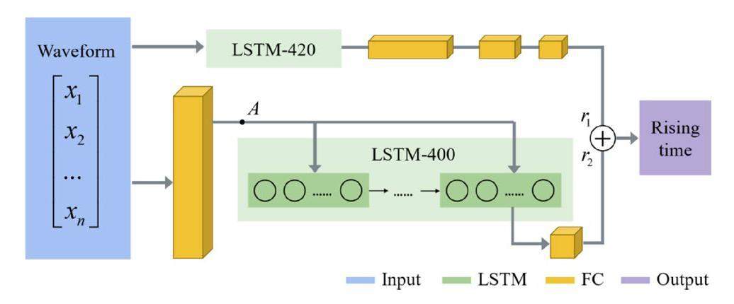
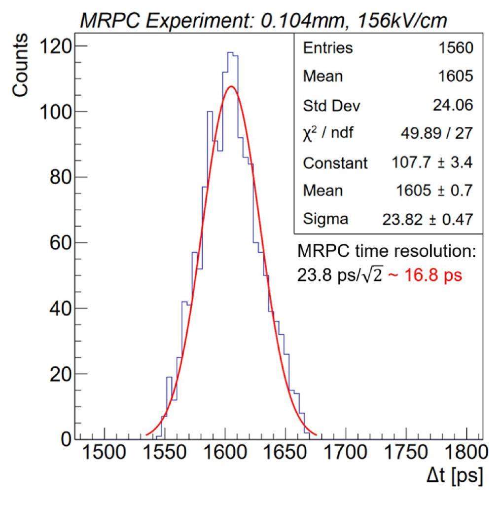
Summary
This work reviews the main characteristics and developments of MRPC for TOF systems. With the improvement of beam energy, intensity and the requirement of particle identification, performance of the MRPC has been developed from the initial ∼ 100 ps resolution and < 1 kHz/cm2 rate capability, to a level of 16 ps and 70 kHz/cm2. Great efforts have been made on the detector physics, materials, electronics, and time reconstruction methods. It is believed that MRPC with higher performances will continue to show up, promoting the application of MRPC to modern high energy physics experiments.
In addition to the research on the time resolution and the rate capability, there are other issues and frontiers that attract much attention in recent years:
1. Find ecological gas substitutes. As mentioned, the environmental impact from the operation of large MRPC-TOF systems must be eliminated. Related works have started for large experiments such as ATLAS and CMS [300, 301];
2. Application to industry and health care. With excellent time and position resolution, MRPC shows potential as futural detectors in technologies like PET [302, 303] and muongraphy [304];
3. Fast waveform sampling techniques. The readout chain with high precision waveform sampling is proved to be essential for reaching the extreme time resolution of MRPC. Nowadays SCA and FPGA technologies are the feasible solutions as next-generation electronics [305]. In the future new technologies and better performance may emerge with unremitting work.
Scintillation Detector
Introduction
A scintillation detector is a type of radiation detector that utilizes the scintillation phenomenon to detect and measure ionizing radiation. The basic principle of a scintillation detector involves the interaction between ionizing radiation and a scintillating material. When a particle strikes the scintillator, it imparts energy to the atoms or molecules within the material, causing them to become excited. As these excited states return to their ground state, they release energy in the form of visible or ultraviolet light. This phenomenon is referred to as scintillation, and the emitted light is proportional to the energy deposited by the incident radiation, enabling the detector to measure the radiation’s energy or dose. The emitted scintillation light is then collected and detected by a photosensitive device, such as a photomultiplier tube (PMT) or a photodetector (PD).
Scintillation detectors come in various material types, each with its unique properties and suitability for specific applications. The scintillation detectors can be classified into inorganic and organic in terms of chemical composition, and also be categorized as solid, liquid, and gas detectors in terms of its physical form. The choice of scintillating materials requires a comprehensive consideration of various performance factors and the specific requirements of the application, such as light yield per MeV, response time, density and atomic number, radiation hardness and cost.
The efficiency of light collection is essential to the overall performance of a scintillation detector, and the optimized light collection helps to improve the detector’s energy resolution and time response. Scintillators are typically surrounded by reflective coatings or films to prevents light from escaping and enhances light collection efficiency. The photon detector, which convert incident photons into electrons and perform electron multiplication processes to enhance signal readout, are either directly attached to the scintillator using optical adhesives or connected via wavelength-shifting optical fibers. Commonly used light detection devices include PMTs, Silicon Photomultipliers (SiPMs), and Avalanche Photodiodes (APDs). The choice of a specific light detection device must match the property of scintillator such as the dynamic range and emission spectrum of photons, and whether the detector is placed in magnetic field.
The sensitivity, accuracy and rapid time response of scintillation detectors make them indispensable tools for a wide range of applications, from nuclear physics and medical imaging to environmental monitoring and security screening.
Electromagnetic Calorimeters In Experiments Of High Energy Physics
In calorimetry, scintillating detectors are employed to measure the energy of particles generated in high-energy collisions or nuclear interactions. The intensity of scintillation light is directly proportional to the energy deposited by the incoming particle. By measuring the amount of emitted light, calorimeters can precisely determine the particle’s energy. This information is vital for understanding the dynamics of particle interactions, identifying specific particles, and probing for new physics phenomena. Scintillating detectors within calorimeters are crucial in high-energy physics experiments and are instrumental in the discovery of new particles and the study of fundamental forces.
Introduction of Electromagnetic Calorimeter
Electromagnetic Calorimeter [306] is a specialized and critical technique used to measure the energy of high energy particles in particle physics, such as electrons and photons, as they interact with and pass through a detector in high-energy physics experiments. The accurate determination of particle energies is fundamental to understanding the properties of particles, the dynamics of particle interactions, and the search for new physics phenomena beyond the Standard Model.
In the realm of particle physics, calorimeters are designed to capture and quantify the energy deposited by charged and neutral particles in the form of electromagnetic showers and hadronic cascades. These detectors play a central role in experiments conducted at particle accelerators like the Large Hadron Collider (LHC) [307] at CERN, Fermilab’s Tevatron [308], and other high-energy physics facilities worldwide.
Particle physics calorimeters are characterized by their high precision, large coverage, and ability to withstand extreme radiation and particle fluxes. They are typically composed of layers of dense and scintillating materials, which emit light when charged particles traverse them. The emitted light is then detected and converted into electrical signals for analysis.
Electromagnetic Interaction Of Particle With Material
The electromagnetic shower begins when a high-energy electron or gamma ray enters a dense material, such as a calorimeter detector or the Earth’s atmosphere, the electron primarily loses energy through Bremsstrahlung radiation, producing photons, as shown in Fig. 67. If the energy of these produced photons exceeds twice the rest energy of the incident electron 2mec2, they can convert into electron-positron pairs through interactions with atomic nuclei. If the generated electron-positron pairs have energies greater than a critical energy Ec, in turn, they can undergo Bremsstrahlung radiation. As the depth of penetration increases, these processes iterate, and the initially high-energy electron or photon gradually transforms into numerous low-energy electrons and photons. This phenomenon is known as the electromagnetic shower process, an electromagnetic shower in GEANT4 is shown in Fig. 68.
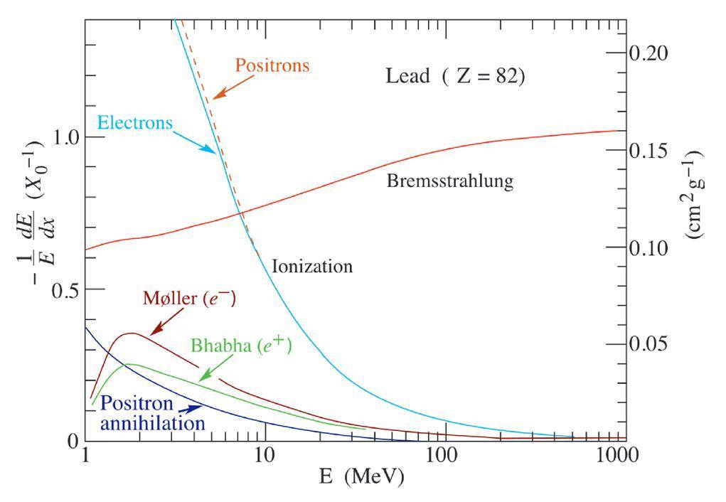
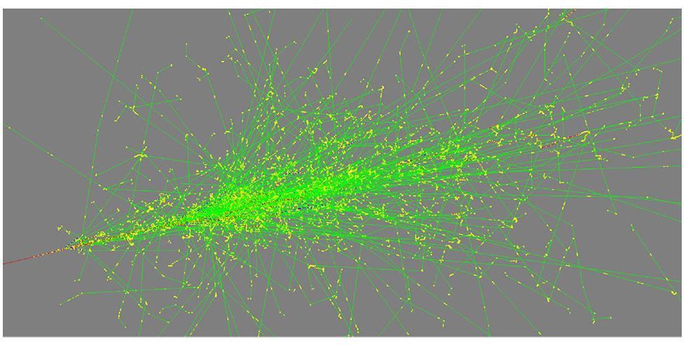
The critical energy Ec is defined as the energy of electron when energy loses by bremsstrahlung is equal to ionization loss. The critical energy Ec is approximately given by [309]:
To describe the transverse spread of an electromagnetic shower in a calorimeter, which mainly due to multiple scattering of electrons and positrons, Molière radius is introduced. It’s defined as the radius of transverse size containing approximately 90% of the energy of the electromagnetic shower. RM can be approximated by [309]:
The energy resolution (σE/E) is the key parameter of a calorimeter, and determines the accuracy of incident particle energy measurement. It improves with increase of energy, and could be written as [309]:
Techniques Of Calorimeter And Application In Experiments
There are two main techniques of calorimeter style: homogeneous calorimeter and sampling calorimeter. The homogeneous calorimeter has only one dense material that have both absorbing and sensitive property. The sampling calorimeter has at least two material in which the material that produces the particle shower as absorber is distinct from the material that measures the deposited energy. The generally used absorber is lead and iron, and the sensitive material is scintillator.
Each technique has its advantage and drawback. Since the homogeneous calorimeter measure all the energy deposited in calorimeter, which means low stochastic term a in Eq. (4), it has a better resolution than sampling calorimeter. However, the homogeneous calorimeters, such as inorganic crystals, are more expensive and constrained in shape and maximum size. On the other hand, sampling calorimeters are cost-effective and can be tailored easily to various shapes based on specific requirements, such longitudinal and lateral segmentation, and therefore they usually offer better space resolution and particle identification than homogeneous detectors.
Homogeneous Calorimeters Homogeneous calorimeters broadly divided into four types that characterized by its material [310]: semiconductor, Cherenkov, scintillation and Nobel-liquid calorimeter. These different types vary in their construction, sensitivity, and application, but the entire detection volume made of a uniform material ensure complete absorption and precise measurement of incident particle energies. Here we will introduce the undoped CsI scintillation calorimeter in Mu2e experiment as an example, and it has good energy resolution and fast response time that works for electron detection with high pile-up.
The Mu2e experiment [311-313] at Fermilab searches for the charged-lepton flavor violating (CLFV) [314] process of a muon-to-electron conversion in an 27Al nucleus field:
The Mu2e calorimeter is comprised of an array of undoped CsI crystals organized into two annular disks (see Fig 69), with front-end electronics positioned on the rear of each disk, and voltage distribution, slow controls, and digitizer electronics mounted in crates. Each disk has an internal (external) radius of 374 mm (660 mm) and is filled with 674 (34 × 34 × 200) mm3 CsI crystals. Each CsI crystal [315] features a transverse dimension of 34 mm×34 mm and a length of 200 mm, and the readout is done by two large-area SiPMs. Notably, to capture the fast scintillation peaked at 310 nm in CsI, the calorimeter utilizes UV-extended SiPMs and inserts a band-pass filter to eliminate the slow scintillation light peaked at 450 nm. The front-end electronics (FEE) comprises two discrete and independent chips (Amp-HV), and provides the amplification and shaping stage, local linear regulation of the bias voltage, the monitoring of current and temperature on the sensors and pulse tests.
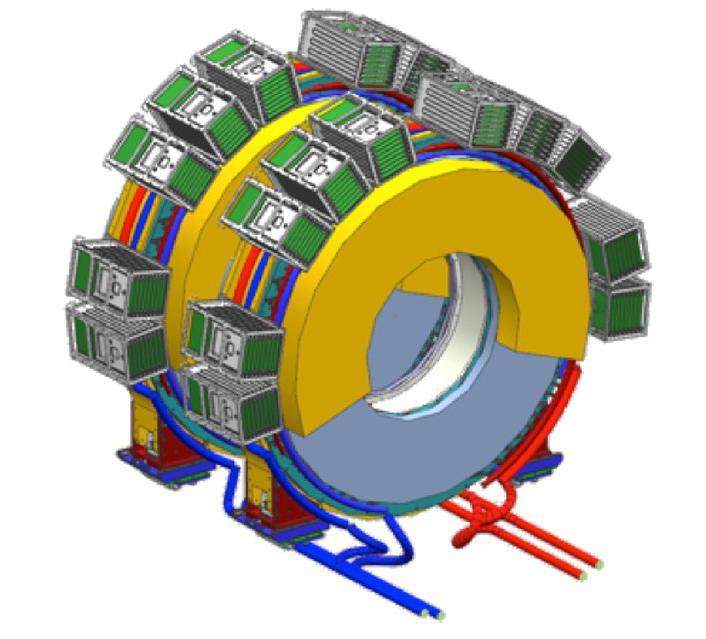
The test results [312] of a large-sized prototype in the Mu2e calorimeter, dubbed as Module0, show that the time resolution at 100 MeV electrons is better than 120 ps, and at 22 MeV (energy deposited by a minimum ionizing particle in a CsI crystal) is 250 ps. The energy resolution of electrons is about 7%, mainly influenced by the shock leakage and beam energy spread.
Sampling Calorimeters The sampling calorimeters have typically have the energy resolution 5–20%/
The KOPIO experiment [313-315] in Brookhaven National Laboratory (BNL), aimed at measuring the branching ratio of the very rare decay model [316] for K
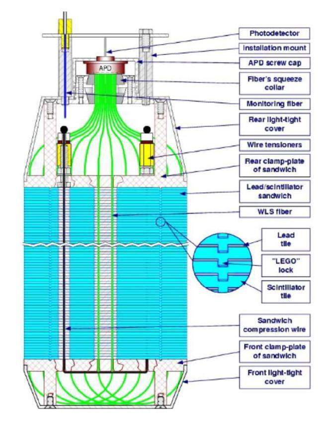
The calorimeter applies the "LEGO"-type locks to improve module’s mechanical property. The lock maintains an air gap between scintillator and lead, and removes 600 paper tiles to reduce effective radiation length from 4 cm to 3.5 cm and the insensitive area from 2.5% to 1.6%. To improve light collection efficiency, a new BASF143E-based scintillator is used in the sampling calorimeter. This scintillator has a high light reflection efficiency of 97% from its surface. In addition, with the BASF143E-based scintillator, the effective light yield in the Shashlyk module (at the entrance to the photo-detector) is 60 photons per MeV.
Based on photon beam test [313], the KOPIO Shashlyk calorimeter employed the APD+WFD readout can reach the energy resolution:
New Techniques And Trend Of Calorimeters
Current improvements in electromagnetic calorimeters are mainly focused on three aspects [310, 320, 321]: time measurement, materials and dual readout (DRO). The time resolution at the level of 10 ~ ps or better will allow the electromagnetic calorimeters to improve the performance of shower reconstruction, energy correction, particle identification and so on. Precise timing data can be collected by all calorimeter cells or a specialized timing layer integrated in the electromagnetic calorimeter to achieve high resolution for the smallest ionizing particles.
Calorimeter materials are divided into inorganic scintillators and organic plastic scintillators. Inorganic scintillators are characterized by fast decay time, with the commonly used inorganic material BaF2 which has a decay time of 0.5 ns. Organic scintillators, such as plastics [322], pure liquid scintillators (LS) [323], and water-based liquid scintillators (WbLS), exhibit fast pulse response (1 ∼ 2 ns) and adequate light yield (104 photons/MeV). When coupled with SiPMs readouts, plastic scintillators are widely utilized due to lower cost, ease of use and flexibility. LS and WbLS are insensitive to radiation, possess long optical transparency, and can be deployed in high-dose environments.
In the DRO method [324], Cerenkov light is used to estimate the electromagnetic component of the shower, and the relative amount of Cerenkov and scintillation light is used to correct the energy of each shower. DRO can be added to a homogeneous calorimeter in two ways: using two filter + SiPM assemblies (sensitive to Cerenkov or scintillation light) at the rear of the crystal; or developing different time structures for fast emission of Cerenkov light and slow emission of scintillation light. Recently, the development of uniform crystal ECAL with DRO has become possible due to the availability of SiPMs with good sensitivity in the red portion of the spectrum. In the long run, research on new optical materials, such as photonic crystal fibers, quantum dots, and semiconductor nanoparticles wavelength shifters, as well as fibers that maintain polarization information, can improve performance and/or reduce the cost of DRO fiber calorimeters.
Scintillators in High-energy Astroparticle Physics
The mechanisms of origins, acceleration and propagations of high-energy Cosmic Rays (CRs) are focused in astroparticle physics and provide an opportunity to reveal the galactic high-energy activities. In the past few decades, the scintillator detectors are broadly applied in the field of astroparticle physics. In 1970s, the NaI(Tl) and CsI(Na) crystals were used to observe the keV level X-rays and gamma-rays in high-altitude space flying by balloon [325-327]. With the development of the technique of space science in recent years, some large-scale direct CRs observation have been carried out internationally, such as the Fermi-LAT [328], PAMELA [329], CALET [330], and etcetera.
The Dark Matter Particle Explorer (DAMPE, also known as “Wukong” in Chinese) is a satellite-born, calorimetric-type, high-energy particle detector [331, 332]. Mainly, one of its scientific objectives is to study the origin, propagation, and acceleration mechanisms of Milky-Way particles by precisely measuring the spectra of high-energy electrons, gamma rays, and nuclei in space. Particularly, the fine structure of the spectrum of electrons and positrons may indicate the processes of dark-matter particles’ annihilation or decay. The DAMPE instrument consists of four sub-detectors as shown in Fig. 71, from top to bottom, a plastic scintillator detector (PSD) [333-335], a Silicon Tungsten tracKer-convertor detector (STK) [336], a Bismuth Germanium Oxide (BGO) imaging calorimeter [337, 338], and a Neutron Detector (NUD) [339].
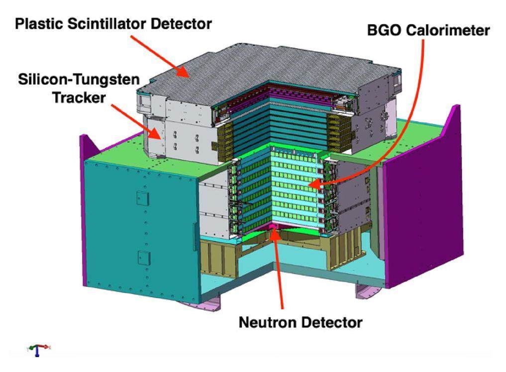
To precisely inspect the spectra of CRs at energy up to ∼ TeVs range, the discriminative separation of incident particle species and accurate measurement of particle’s energy are therefore important. Typically, the organic plastic scintillator detector is used to measure the charge of incident particle or/and as an anti-coincidence of gamma-ray measurement, the inorganic scintillator crystal is composited as a total absorption calorimeter or sampling calorimeter to measure the deposited energy of incident particle. This kind of combination is well adopted by many experiments. The DAMPE detector will be introduced as an example of application of scintillator in astroparticle physics.
The PSD consists of two modules of 41 plastic scintillator strips. Its main purpose is to provide charged-particle anti-coincidence for the gamma ray detection and to measure the charge of charged particles. The PSD has a good charge resolution of about 0.06 e for singly charged particle, and Fig. 72 shows the capability of charge reconstruction for
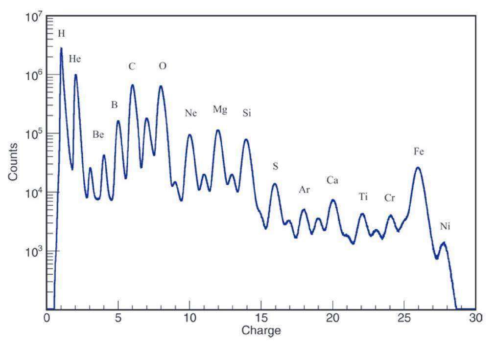
The BGO calorimeter consists of 14 layers of 22 BGO crystals with a dimension of 25 mm × 25 mm × 600 mm shown as Fig 73. To realize a function of three-dimensional imaging, the adjacent layers are organized orthogonally, with a total depth of about 32 radiation lengths and about 1.6 nuclear interaction lengths [342]. As a key component of DAMPE detector, the BGO calorimeter measures the deposited energy of incident particle, containing > 90% kinetic energy of electromagnetic cascades with the resolution better than 1.2% for energies exceeding 100 GeV [331, 337]. The electron/proton discrimination method relies on the topological differences of shower shape between the electromagnetic and hadronic particles in the detector. Thanks to the excellent capability of three-dimensional imaging, together with the selection procedures, the BGO calorimeter can reject larger than 99.99% protons while analyzing the electrons. Figure 74 shows the discrimination power of BGO calorimeter between electrons and protons at the energy range of 500 GeV-1 TeV [343].
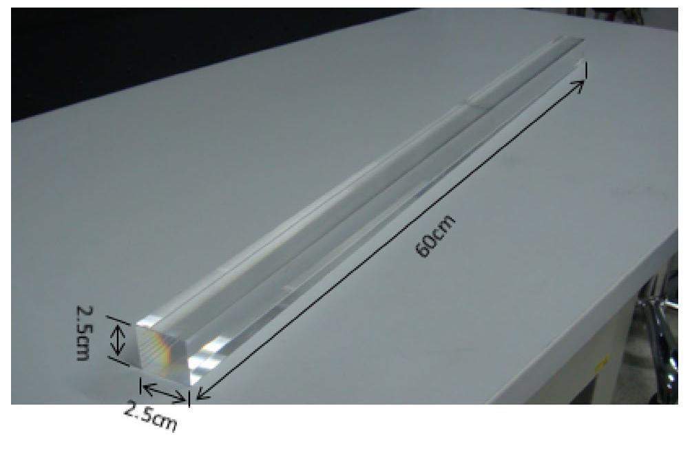
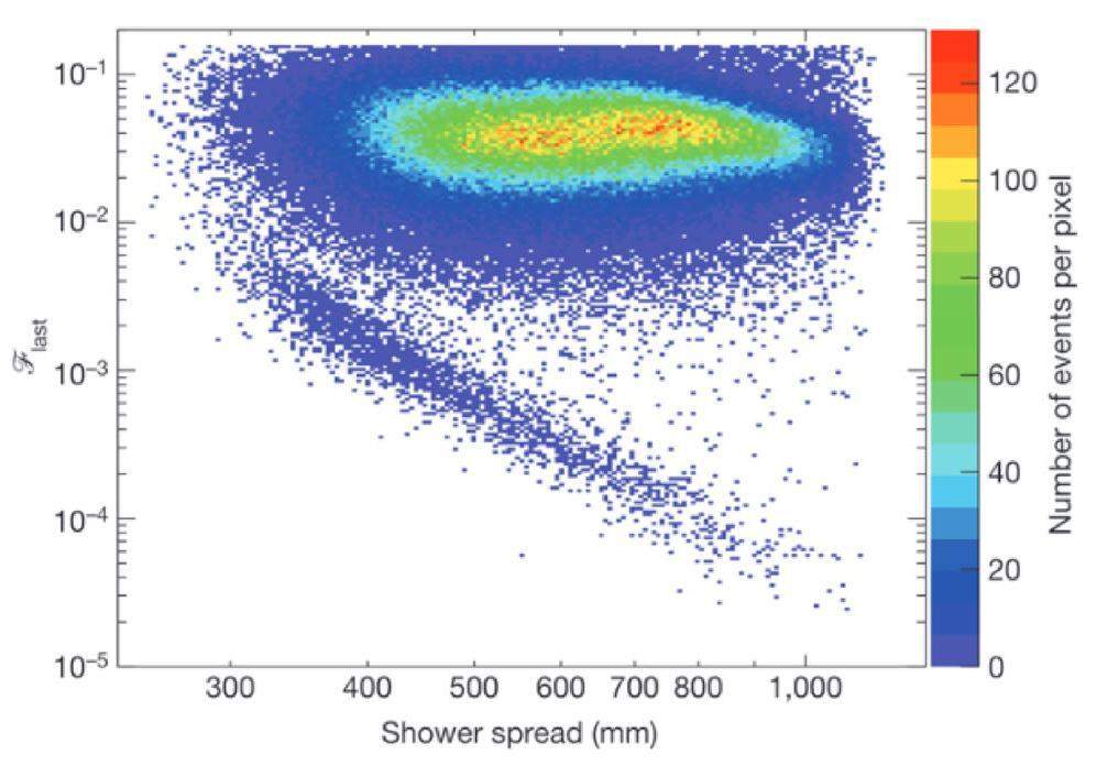
The DAMPE has been working on-orbit for nearly eight years since it was launched into a sun-synchronous orbit at an altitude of about 500 km on 17 December 2015. As a high-energy particle detector, except collecting CRs above GeV level, DAMPE also faces a severe environment of space radiation of low-energy trapped particles from Van Allen belts [344, 345]. High-quality statistics relies on stable performance of the detector, of which the energy measurement is especially important during such a long-time operation.
The attenuation length λ which is defined as the propagation length that the number of photosreduced by a factor of e is an essential character of scintillator. The attenuation length of the 600 mm BGO crystal is calibrated and the result is shown in Fig. 75 [346]. The decrease of the attenuation is generally steady as a function of time. And the variations are applied to the correction of energy reconstruction. When it comes to the energy reconstruction, the absolute energy scale and the quenching factor become two important parameters to be considered. The Minimum Ionizing Particles (MIPs) deposit energy almost the same when passing the certain length[347] and the quenching effect is found non-negligible for nuclear charge Z>6 [348]. Thus, 14-layer proton MIPs and one layer carbon MIPs are selected to evaluate the stability of absolute energy scale and quenching factor, respectively. The variations of absolute energy scale and quenching factor are shown in Fig. 76 and 77, respectively, with fluctuations of both less than 1%. The energy linearity of energy deposition between the shower maximum crystal and the whole calorimeter has been checked detailly. The good energy linearity ensures the reliability of energy reconstruction and the extension to higher energy range [349].
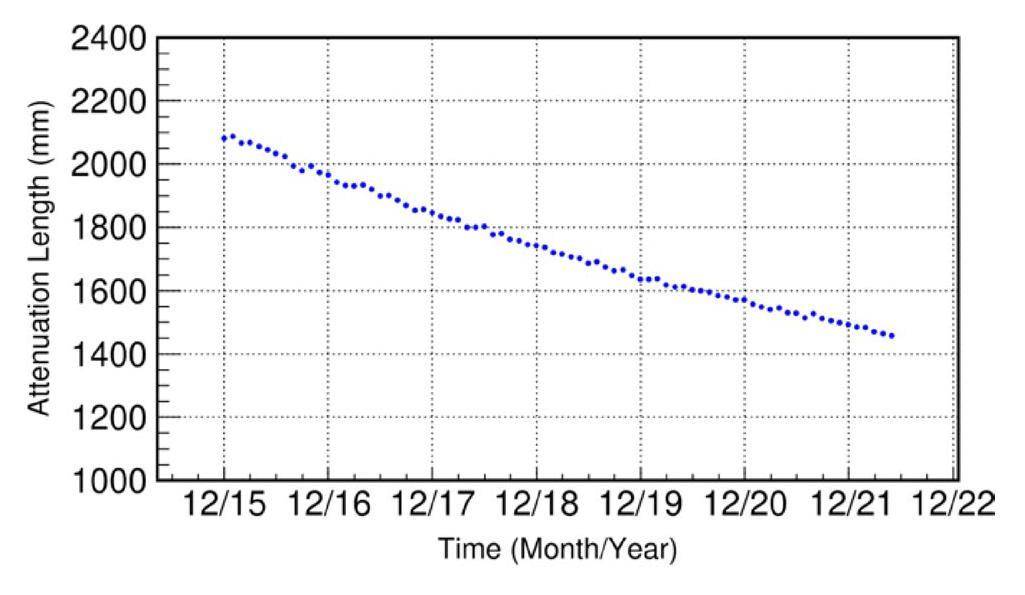
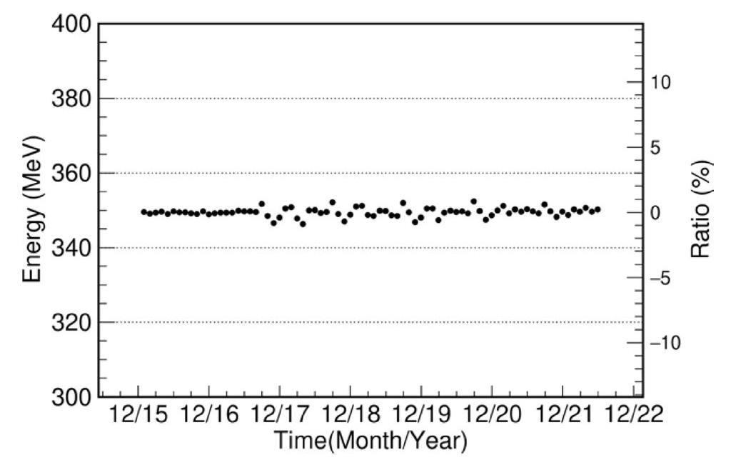
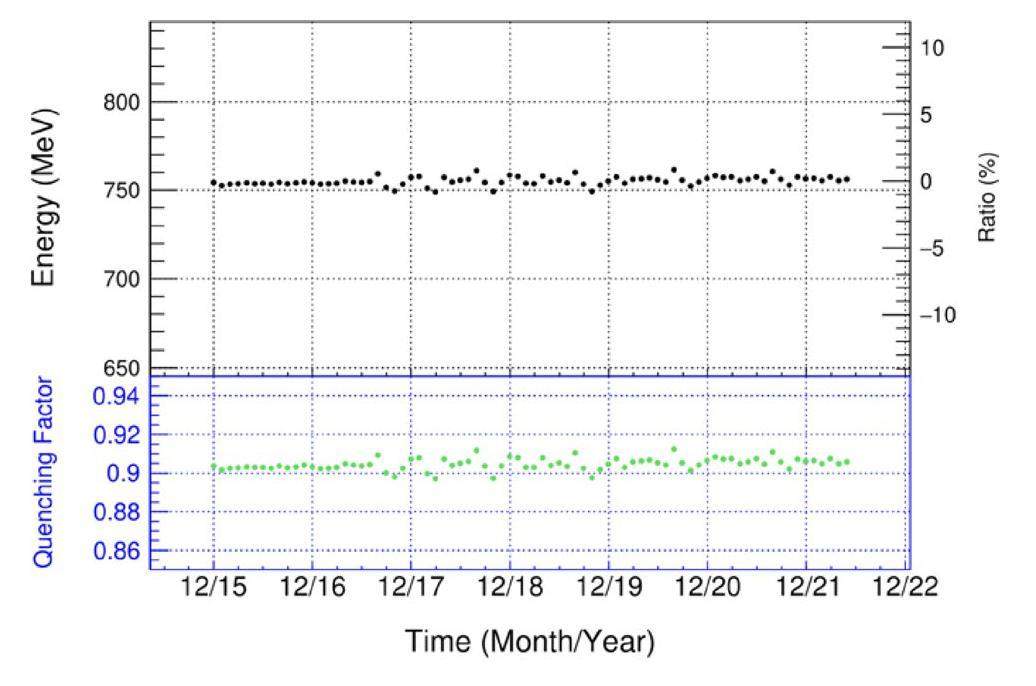
The stability and reliability are clearly illustrated by the performance of DAMPE scintillator detector of PSD and BGO calorimeter. There are also many other experiments use scintillators such as LYSO, PWO, CsI [350], etc. To measure the energy spectra of high-energy particles in space, the inorganic scintillator is undoubtly a good choice to composite the full absorbing calorimeter and the organic plastic scintillator provide an accurate identification of particle’s charge.
Cosmic Ray Muon Imaging
Cosmic ray muon imaging, also known as muography, is an emerging technology with significant potential. It discriminates different Z materials and offers advantages for non-destructive deep detection of large targets. Additionally, there are no potential risks associated with artificial radiation sources. Consequently, detection systems, algorithms, and applications for muography have been developed and implemented in various scenarios.
One of the most common design schemes for detectors involves using plastic scintillators. Plastic scintillator has the advantages of high detection efficiency, robustness, easy maintenance, and low cost. Hence, plastic scintillator has become a good option for building muography detectors in various field scenarios, especially in tough environments such as mines.
The typical muography detection systems based on plastic scintillator are the Lanzhou University Muon Imaging System (LUMIS, as shown in Fig. 78) [351, 352], and Cosmic Ray Muon Imaging System (CORMIS, as shown in Fig. 79) [353] from Lanzhou University. These systems utilize triangular prism scintillator bars coupled with Si-PM chips for detection. Thirty-two scintillator bars are arranged in a detection plane (as shown in Fig. 80 (a)). Scintillating lights emitted upon muon interaction are detected by Si-PM chips. Front-end electronics nearby amplify and digitize pulses coming from Si-PM chips above thresholds. Digitized data is sent to a master board for a coinciding purpose and then transferred to a personal computer for storage and further analysis. One detector plane provides a one-dimensional coordinate of a muon hit. Another plane, stacked over and oriented orthogonally, provides the other coordinate of the hit. Such a pair of orthogonal planes is called a super plane. Using two pairs of such super planes separated by a certain distance allows for evaluating the direction of muons in three-dimensional coordinates.


LUMIS consists of 4 super planes divided into two muon trackers. The upper tracker records the incident trajectory of muons, while the lower tracker records the outcoming trajectory of muons below the imaging area. This configuration can measure the muon scattering angles, thus probing different Z materials based on muon scattering measurements. The experimentally test on the prototype of the LUMIS system in muon scattering imaging demonstrated that each detection plane achieved up to 98% detection efficiency, with a position resolution of 2.5 mm. The angular resolution of two super planes is 8.73 mrad at a spacing of 40.5 cm. Three-dimensional reconstructions from experimental scattering data correlated with the profile of a test lead brick sample (as shown in Fig. 81).

CORMIS is used mainly for muon absorption-based imaging to probe the density distribution inside large-scale objects. It consists of 2 super planes measuring directional muon counting rates and directional survival rates. Then, the survival rates are propagated to directional effective lengths that are inverted to a 3D density distribution.
The first muography application for a large-scale cultural relic (the Xi’an City Wall) in China utilizes CORMIS. High-quality three-dimensional density distribution was obtained through strategic position selection, data statistics, hypothesis testing analysis, and two inversion procedures. Figure 82 shows the measurement position and the internal density anomalies discovered in the result. This achievement received significant media coverage and highlighted the successful application of muon tomography in cultural heritage preservation.
Another pioneering application of muography was carried out in the Zaozigou Gold Mine, focusing on low-density-contrast ore bodies. After roughly half a year of measurements using six CORMISs, the muography result reconstructed a gold orebody, a limonitic siliceous slate structure, and several mined-out areas (as shown in Fig. 83). The results demonstrated the sensitivity of muography for distinguishing slight differences in density. The application in Zaozigou Gold Mine is the first muography application in minerals in China, emphasizing the tremendous potential value of muography in the economic, research, and safety aspects of mineral exploration and inspection work.
Also, a compact small-diameter borehole-type detector has been proposed and studied.. The detector utilizes a dual-end readout configuration of CsI(Tl) scintillators [354], forming the position-sensitive detector (PSD). The design incorporates square cross-section scintillators to maximize interior space utilization (as shown in Fig. 84). Experimental results demonstrated that the PSD achieved a position resolution of 5.1 mm. Monte Carlo simulation estimated an azimuthal resolution of 0.103 rad and a zenith angle resolution of 0.016 rad. The development of borehole-type detectors opens up possibilities for future muography applications underground.
Neutron Detection
Scintillators can aslo be used to detect neutrons. The shape of the resulting light pulses provides information that can help differentiate between neutron and gamma interactions. This subsection will presents the neutron detection based on inorganic scintillators and organic scintillators.
A scintillator is a device that can be used to detect neutrons [355-357]. The scintillation material is typically made of an inorganic crystal or a liquid organic compound. When a neutron interacts with the material, it transfers energy to the atoms, causing them to become excited. These atoms then release the excess energy in the form of light photons. The emitted light is typically in the ultraviolet or visible range. The photodetector, such as photomultiplier (PMT) tube, silicon photomultiplier (SiPM) and photodiode, is placed in close proximity to the scintillation material to capture the emitted photons and convert them into electrical signals, which can be analyzed and measured. The shape of the resulting light pulses provides information that can help differentiate between neutron and gamma interactions.
Inorganic Scintillators
Inorganic Scintillators Containing 6Li Typical inorganic scintillators containing 6Li include Li glass, LiI(Eu), LiF/ZnS:Ag, and potassium cryolite crystals. Li glass detectors can measure neutrons below several hundred keV with high detection efficiency, but they have low light yield and are also sensitive to γ [358]. LiI(Eu) scintillators, on the other hand, can measure neutron energy spectrum in the MeV range, but with poor resolution and low light yield. Recent studies have shown that appropriate doping levels and thermal treatment of pure LiI crystals doped with Eu2+ can address the light yield issue in LiI(Eu) for neutron detection, and improve its energy resolution and n/γ-discrimination capability to some extent [359]. LiF/ZnS:Ag, which exhibits excellent n/γ-discrimination characteristics, necessitates thin detectors due to the low transparency of ZnS(Ag), resulting in lower detection efficiency [360]].
Potassium cryolite materials, as a newly developed type of inorganic scintillator, are considered as potential alternatives to LiI(Eu). Various derived products have been developed in recent years, including Cs2LiYCl6:Ce (CLYC), Cs2LiLaCl6:Ce (CLLC), Cs2LiLaBr6:Ce (CLLB), Cs2LiLaBr6-xClx:Ce (CLLBC), Cs2NaYCl6 (CNYC), Cs2LiYBr6:Ce (CLYB), etc. Potassium cryolite materials exhibit high light output (>20000 photons/MeV), good energy resolution (Eγ = 662 KeV, < 5%), and excellent n/γ discrimination capability [361]. However, they have some limitations in the detection of fast neutrons[362]. A. Gueorguiev and others have developed a new technology that combines inorganic scintillator (CLYC) with an organic scintillator matrix (methyl methacrylate, PMMA) to achieve simultaneous detection of fast neutrons, thermal neutrons, and γ-rays. Fig 85 illustrates the structure of this composite detector [363].
Inorganic Scintillators Containing 10B The latest developments involving scintillators containing 10B are primarily focused on neutron imaging. In 2014, Nakamura developed a low-afterglow, thermal neutron-sensitive ZnS/10B2O3 scintillator with a decay time of 60 ns, which offers potential for neutron imaging [365]. In 2020, Miller conducted neutron imaging research using a 10B/Cs(Tl) scintillator screen, directly depositing 10B onto Cs(Tl) thin film using electron beam deposition to create a layered scintillator structure, enabling a spatial resolution of 9 μm [366]. Additionally, William found that boron-based scintillators exhibit excellent neutron detection capabilities in applications involving cold and ultra-hot neutrons, making it highly likely to achieve higher-quality neutron images with shorter imaging time [364].
Organic Scintillators
Organic scintillators, rich in light elements such as H and C, are commonly utilized for neutron detection using the nuclear recoil method. Organic crystals, liquid scintillators, and plastic scintillators all fall under the category of organic scintillators. They have short decay times for light emission, often on the order of tens of nanoseconds, making them suitable for high neutron flux detection. However, organic scintillators generally exhibit sensitivity to gamma rays as well.
Organic Crystals Anthracene and stilbene crystals are the basic types of organic crystals used for fast neutron detection. These two crystals have high light yields and good discrimination capabilities between neutrons and gammas. However, they exhibit anisotropic light response and significant temperature effects. Additionally, it is challenging to obtain crystals with large size and high cost. In the first decade of this century, a team led by Natalia Zaitseva at Lawrence Livermore National Laboratory (LLNL) in the United States developed new crystal growth methods [367]. The new crystal growth methods developed by the team at LLNL allowed for the production of larger and more uniform organic crystals, addressing the previous challenges in obtaining large crystals. These advancements in crystal growth have contributed to an increased interest in organic crystals for various applications, including fast neutron detection.
Liquid Scintillators Liquid scintillators are also used for fast neutron detection. However, their solvents mainly consist of flammable and toxic substances such as toluene, xylene, and trimethylbenzene. Therefore, extra caution is required during their use to prevent incidents such as breakage, leaks, or flash explosions. The conditions for using liquid scintillators are more demanding and strict in order to ensure safety.
Plastic Scintillators Plastic scintillators have higher detection efficiency for fast neutrons compared to other detectors. They are also cost-effective, high mechanical strength, and can be processed into various shapes, making them suitable for use in various harsh environments. However, plastic scintillators cannot be used for thermal neutron measurements, and most commercially available plastic scintillators, except for EJ-276, have poor n-γ discrimination capabilities. Therefore, the development of doped plastic scintillators that have simultaneous detection capabilities for fast and thermal neutrons, as well as improved n-γ discrimination, is one of the current directions in scintillation detector research.
Natalia Zaitseva has produced plastic scintillators with enhanced n-γ discrimination capabilities, surpassing the commercially available EJ-309 liquid scintillator [368]. Figure 86 shows the pulse shape discrimination spectrum of this scintillator compared to EJ-309 for 252Cf. Furthermore, Natalia Zaitseva and others have also developed plastic scintillators containing benzyl salicylate lithium, which exhibit good discrimination capabilities for thermal neutrons, fast neutrons, and γ-rays[369]. Figure 87 neutron energy range.
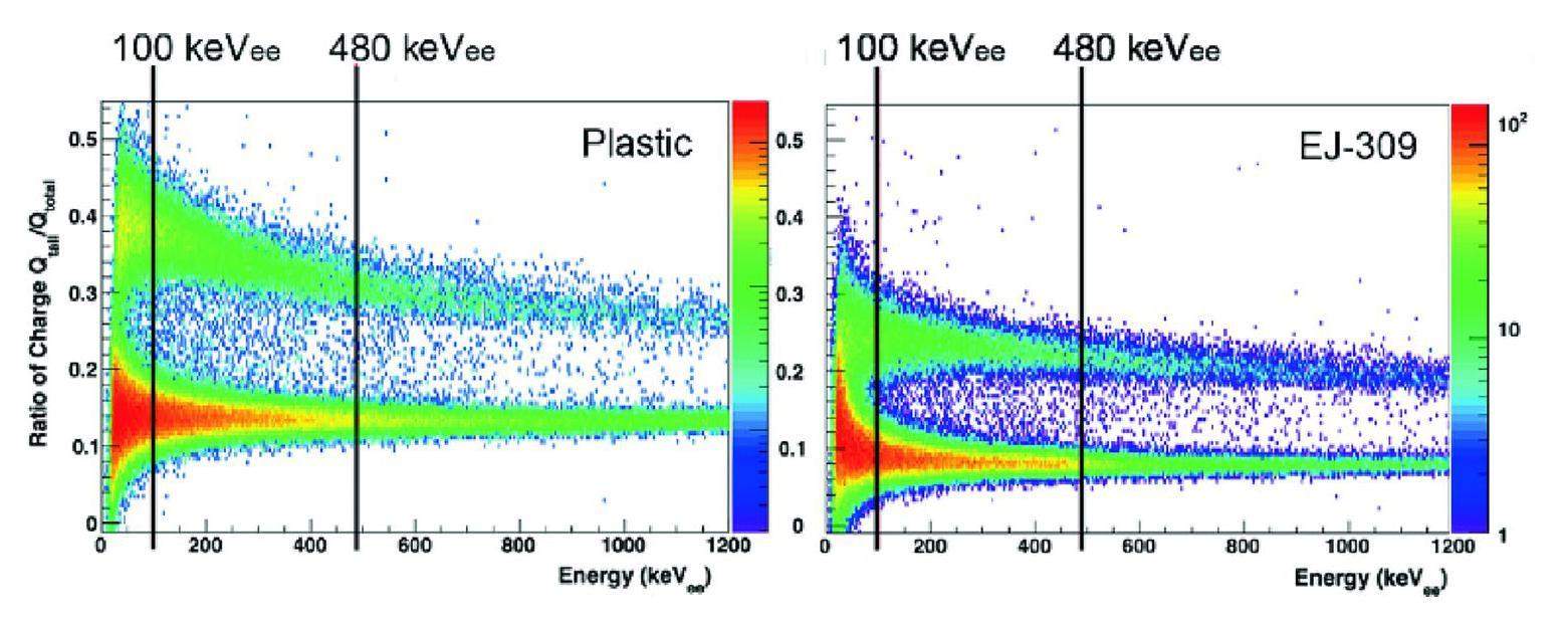
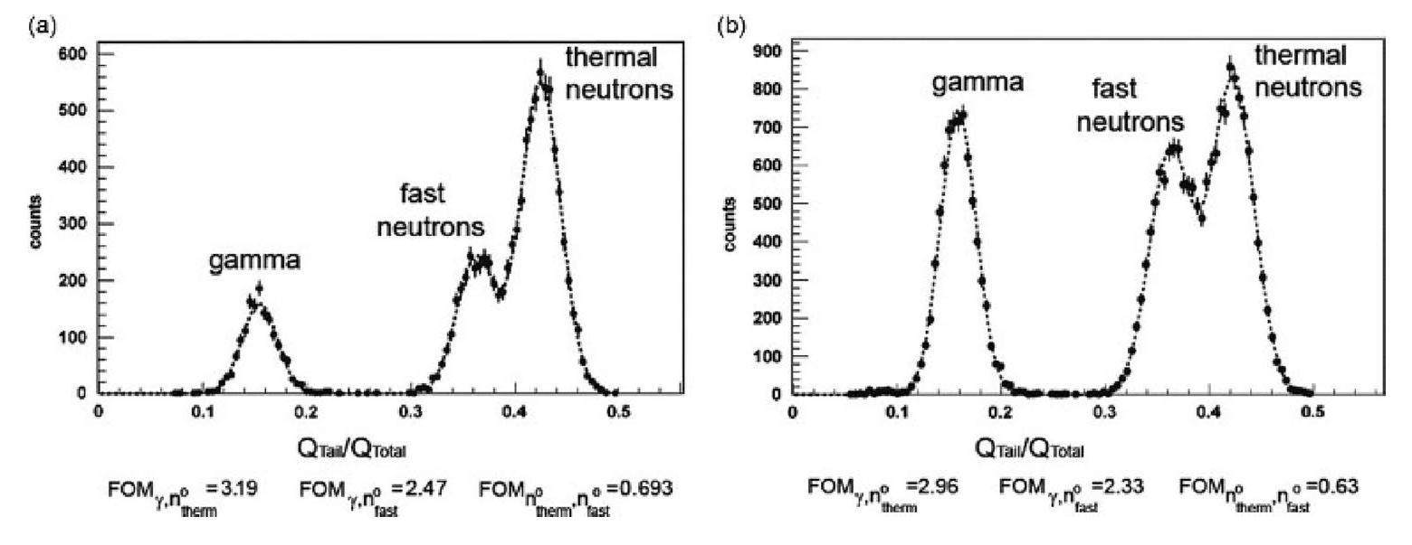
Cherenkov Detector
The Principles Of The Cherenkov Detector
A uniformly moving charged particle traversing through a homogeneous medium with a refractive index of n, and with a velocity surpassing the phase velocity of light in the medium c/n, initiates a coherent superposition of electromagnetic radiation emitted during the de-excitation process of the medium’s atoms or molecules. This phenomenon gives rise to the formation of a Cherenkov light cone along the direction of particle motion. The relationship between the Cherenkov radiation angle (θC) and the velocity of the charged particle is expressed as:
Currently, two commonly used Cherenkov detectors have been developed: the Ring-Imaging CHerenkov detector (RICH) and the Detector of Internally Reflected Cherenkov light (DIRC), as illustrated in Fig. 88. RICH detector directly measures the Cherenkov radiation angle excited by charged particles within the radiator material. On the other hand, DIRC detector determines the Cherenkov angle indirectly by measuring the exit angle and time of Cherenkov light after multiple internal reflections within a radiator material, commonly fused silica. The advantages of RICH detector include the ability to discriminate particles over a wide range of momenta by replacing radiators with different refractive indices. However, its drawbacks are the larger volume of the optical imaging system, complex structure, and higher cost. In comparison, DIRC detector features a more compact structure with a thickness typically ranging from 1 to 2 cm, resulting in a smaller spatial requirement for the detector. However, one limitation of DIRC detector is its smaller momentum coverage compared to RICH detector. For instance, the state-of-the-art high-performance DIRC (hpDIRC) in the Electron-Ion Collider (EIC) is expected to achieve a maximum momentum of ∼ 6 GeV/c at 3σ π/K separation [370]. Based on the momentum distribution characteristics of final-state particles produced in electron-nucleon collisions, it is common practice to employ RICH detector in the endcap region and DIRC detector in the barrel region, as exemplified by the design of Belle II [371, 372].
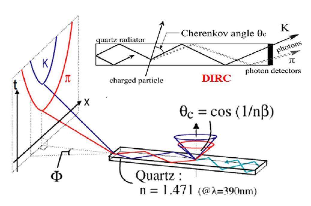
The Development Of RICH
The RICH detector was invented as early as the early 1980s and has been utilized in experiments such as E605 [374], WA69 [375], and WA82 [376]. Following over a decade of development and iterations, the third generation of RICHes, constructed in the mid-1990s, demonstrated outstanding performance in experiments such as SELEX [377], HERMES, and HERA-B. With advancements in novel photodetector devices and high-speed readout electronics, the significance of the new generation of RICHes in high-energy particle physics experiments has become increasingly prominent [378].
HERA-B was an experiment conducted at the HERA electron-proton collider to study B mesons and D mesons produced in the interaction of 920 GeV/c protons with a fixed target. The RICH detector in this experiment utilized C4F10 gas as the radiator, and the spherical mirror was split into two halves, tilted at 9∘ in opposite directions (Fig. 89), to ensure that the photon detector only captured Cherenkov light cones and avoided interference from other particles. The upper and lower photon detector modules of the RICH detector consisted of Hamamatsu R5900-M16, Hamamatsu R5900-M4, and other devices, including a telescope system to enhance the efficient collection of photons [379]. The detector was capable of achieving a 3σ separation for π/K particles with momenta of ∼ 50 GeV/c [380].
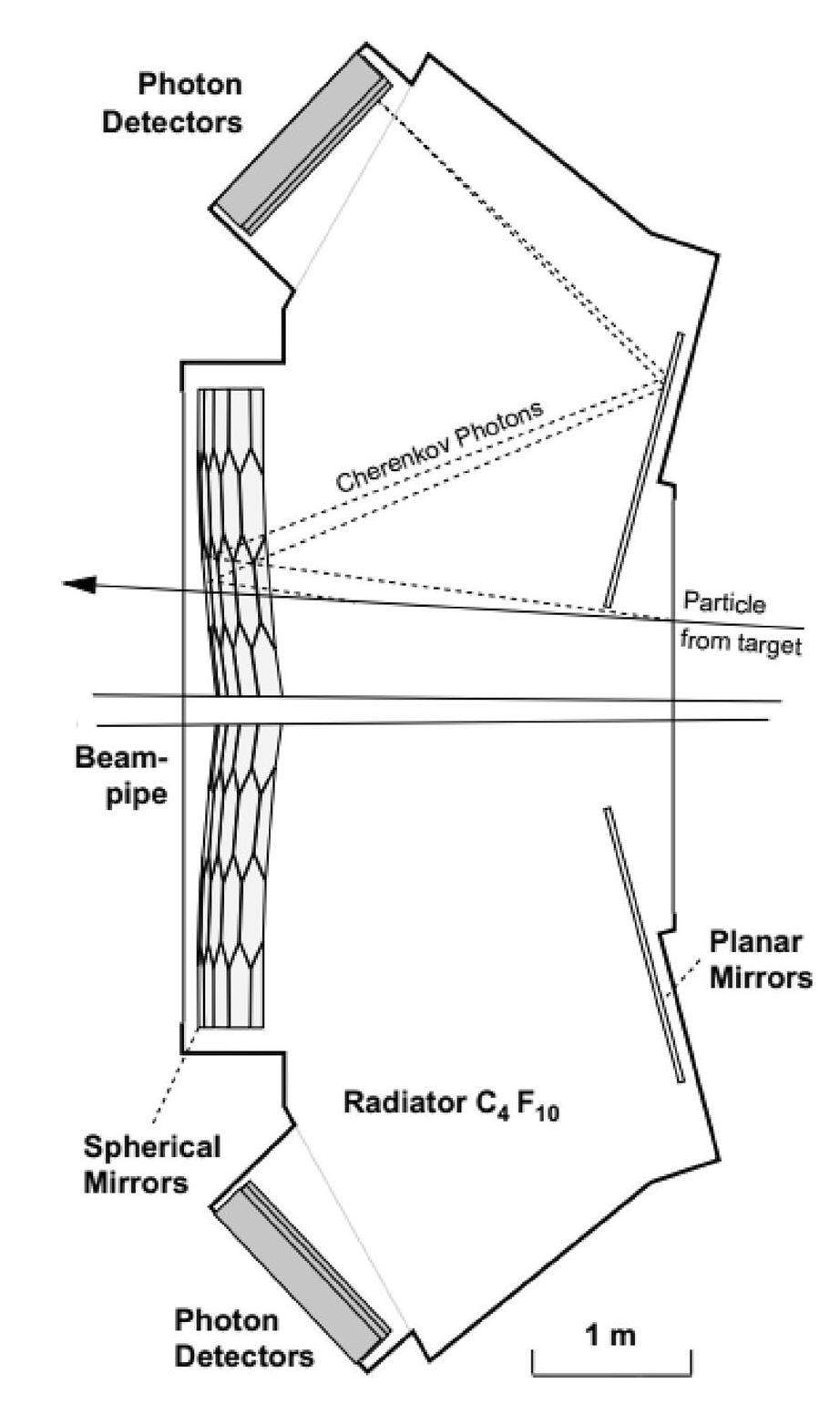
The HERMES experiment employed a dual-radiator RICH (dRICH), utilizing C4F10 gas and a silica aerogel wall to extend the momentum detection range. This configuration enabled the discrimination of π/K/p particles in the momentum range of 2 to 15 GeV [381]. Interestingly, this approach was initially proposed by the LHCb experiment. In LHCb, the RICH 1 detector employed a combination of C4F10 gas and aerogel for particles in the polar angle range of 25 to 300 mrad and momentum range of 2 to 40 GeV/c. RICH 2 detector only used gaseous CF4 for PID in the polar angle range of 15 to 100 mrad and momentum range of 15 to 100 GeV/c[382]. Nevertheless, during its RUN I phase, it was observed that RICH 1 detector couldn’t effectively differentiate particles from these two radiators, and the presence of aerogel reduced the reconstruction rate. Consequently, during RUN II, the aerogel was removed [383]. The photon detectors of the RICH detector utilized the Hybrid Photon Detector (HPD) [384], which was developed in collaboration with Hamamatsu Photonics and specifically designed for the LHCb RICH system. They were subsequently upgraded in 2019-2020 to Hamamatsu’s R13742 MaPMTs and R13743 MaPMTs [385].
The BELLE II experiment, in order to increase photon yield without compromising resolution, adopted a near-focusing RICH scheme with a dual-layer aerogel radiator. This scheme employed aerogel layers for focusing, where the refractive index of the upstream aerogel was slightly lower than that of the downstream aerogel (1.045 and 1.055). The photon detectors, utilizing the Hybrid Avalanche Photo Detector (HAPD) [386] jointly developed with Hamamatsu Photonics, achieve a 3σ separation of π/K up to ∼ 4 GeV/c [387].
The main scientific objectives of the currently under construction EIC involve investigating the spin and flavor structure of nucleons and atomic nuclei, as well as researching Quantum Chromodynamics (QCD) in extreme parton density regimes. It is the world’s first collider with polarized electron and light-ion beams, capable of generating heavier, non-polarized ion beams, up to uranium. As shown in Fig. 90, the electron endcap, hadron endcap, and barrel regions of the EIC employ Cherenkov detectors for PID, specifically utilizing module RICH (mRICH), dRICH, and DIRC [388, 389](see the following section for DIRC details).
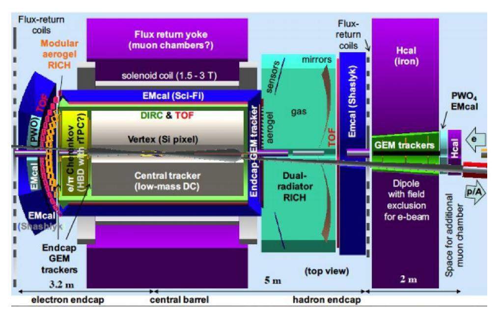
The radiator of the dRICH detector consists of aerogel, C2F6 gas, and an acrylic filter with a thickness of < 300 nm(to absorb the majority of Rayleigh scattered photons generated within the aerogel). This RICH detector is designed for comprehensive hadron identification ranging from 3 to 50 GeV/c (π/K/p), as well as for electron identification up to ∼ 15 GeV/c (e/π).
The mRICH detector not only needs to provide hadron identification capabilities within a momentum range from 3 to 10 GeV/c but also requires a compact design to accommodate the spatial constraints of the EIC experiment. Each mRICH module is self-containing (see left in Fig. 91), encapsulating an aerogel radiator, a focusing Fresnel lens with n = 1.47 refractive index and 6”(15.24 cm) focal length, and pixelated photon sensors within a box of approximately 14 cm × 14 cm × 25 cm. As shown on the right side of Fig. 91, the Fresnel lens focuses photons emitted parallelly by the aerogel to converge at a point with relatively larger angles. This process generates a clearer and more compact Cherenkov ring, thus achieving better separation capabilities without the need for a large photon detection area. The photon detectors for this RICH detector are currently under discussion and evaluation. It is anticipated that the choice will be between the Hamamatsu H13700 and Silicon PhotoMultiplier (SiPM).
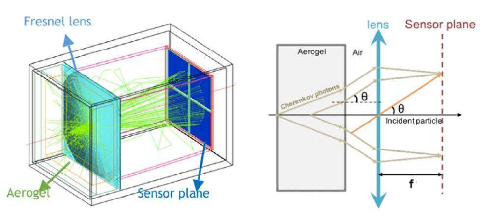
The Development Of DIRC
The DIRC detector was first proposed and successfully implemented by the BABAR collaboration [390]. The DIRC detector structure in the BABAR experiment, as shown in Fig. 92, utilized highly polished, bar-shaped quartz (synthetic fused silica) as its radiator. This material is resistant to ionizing radiation damage, has a long ultraviolet light attenuation length, and exhibits low dispersion within the Cherenkov light wavelength range. To prevent photon loss due to internal reflection at the quartz-water interface and to reduce the required size of the detection surface, the end of the quartz bar is connected to a wedge-shaped quartz light guide. The light guide’s distal end is a water-filled expansion volume, referred to as the Stand-Off Box (SOB). The SOB’s annular surface is equipped with an array of 10752 PhotoMultiplier Tubes (PMTs), along with hexagonal-shaped “light catchers" to maximize the detection area. The PMTs are connected to front-end electronics outside the SOB, comprising a total of 168 DIRC Front-end Boards (DFBs), each processing signals from 64 PMTs.
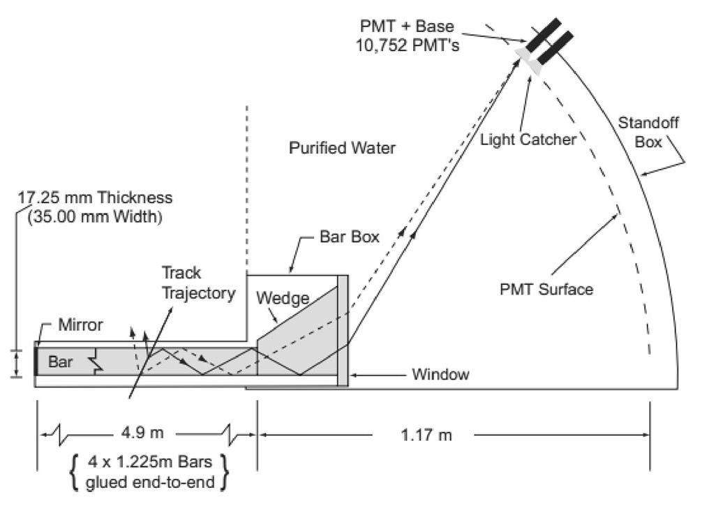
Due to the use of 6,000 liters of ultra-pure water as the light guide medium in the BABAR DIRC, which was sensitive to electromagnetic and neutron backgrounds and also voluminous, the canceled SUPERB project proposed a new structure called Focused DIRC (FDIRC). This system replaced the light guide in the BABAR with a precise optical focusing system, reducing the detector’s volume to 1/25th of the BABAR DIRC and improving the response speed by a factor of 10 [391].
The subsequent BELLE-II experiment developed a simple DIRC-like detector, Time Of Propagation counter (TOP), capable of separating π/K/p under 4 GeV/c. This device placed position-sensitive photodetectors (MCP-PMT arrays [392]) directly at the rear of the bars, precisely measuring the exit position and flight time of photons for three-dimensional image reconstruction (x, y, and time). Although the performance of this design is comparable to that of BABAR’s, it achieves this goal with a very small expansion volume and a compact readout. Furthermore, its radiator used wide bars (plates), significantly reducing costs compared to the thin bars used in BABAR [372].
JLab’s GlueX experiment repurposed some BABAR DIRC quartz bars, along with MAPMTs and electronics from the CLAS12 RICH, to construct the GlueX DIRC. This design also drew inspiration from the FDIRC concept, with the difference being that its radiator used distilled water instead of quartz, and it utilized three planar mirror segments to approximate a cylindrical mirror. This design was capable of achieving 3σ separation of π/K/p up to about 4 GeV/c [393].
The PANDA experiment [394], aiming to address various issues related to strong interactions and planning its first antiproton physics experiment in 2025, features one of the most representative DIRCs. The barrel DIRC detector [371] in this experiment employed a triple-lens system composed of a layer of lanthanum crown glass (NLaK33) and two layers of synthetic fused quartz. This triple-layer lens operated without any air gap, minimizing photon loss during the transition from the lens to the expansion volume. Inspired by the FDIRC, the expansion volume part utilized 16 compact fused silica prisms instead of the large water tank of the BABAR DIRC, making it easier to integrate and less susceptible to harmful radiation from the accelerator. Due to improvements in the lens and expansion volume, the system employs 48 radiators, each 2400 mm long and 53 mm wide, significantly reducing polishing costs compared to BABAR’s. Additionally, developments in electronics have been key to its performance improvements. Its photodetectors used 6.5 mm × 6.5 mm MCP-PMTs, capable of operating in a strong magnetic field (1 T), with a single-photon timing resolution of 30–40 ps and a gain of about 106. Based on TRB3 technology [395] for readout and using the DiRICH system’s front-end electronics, the system achieves a timing precision of 100 ps. Overall, the DIRC works between 22 and 140 and can distinguish π/K below a momentum of 3.5 GeV/c.
The endcap of this experiment also utilized a DIRC, named the Endcap Disc DIRC (EDD) [396]. Although the basic concept of EDD was proposed as early as 1996 [397], it was first realized in the PANDA endcap. The EDD was divided into four independent quadrants, each consisting of a 20 mm thick fused silica radiator disk. Together, these disks form a dodecagon with a diamond-shaped notch at the center. Each quadrant comprises a radiator and 24 ReadOut Modules (ROMs). Each ROM contained three bars, three 16 mm Focusing Element Lenses (FELs), MCP-PMT, and a front-end electronics board. As shown in Fig. 93, the Cherenkov photons emitted within the radiator are ultimately detected by the MCP-PMTs at the edges, allowing for the determination of the Cherenkov angle and azimuthal angle through algorithms.
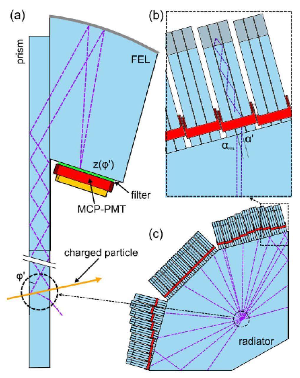
As stated in the previous section, the DIRC will be used in the barrel region of the EIC. This DIRC detector will expand the momentum coverage of the PANDA DIRC, allowing for 3σ separation of π/K, e/π, and p/K at 6 GeV/c, 1.8 GeV/c, and 10 GeV/c, respectively. Its fundamental structure is similar to the PANDA barrel DIRC, with the primary difference lying in its adoption of smaller pixelated photon sensors. Specific aspects related to these photon sensors and reconstruction algorithms are still under discussion and evaluation [370].
Summary
Over the past forty years, driven by the particle identification demands in accelerator-based particle physics experiments, Cherenkov detectors have experienced continuous advancements. These advancements are fueled both by structural innovations, such as dual-radiator structure, DIRC structure, and the optical structure of FDIRCs, as well as by improvements in device performance, including smoother quartz radiators, smaller photon pixel detectors, higher precision timing technologies, and superior image reconstruction methods. Its development has not only contributed to the prosperity of particle physics experiments but has also led to the progress of practical fields such as cosmic ray detection, industrial metal inspection, and medical imaging.
Transition Radiation Detectors
Introduction
Transition Radiation (TR) refers to the electromagnetic waves generated when ultrarelativistic charged particles traverse interfaces between different media. Its existence was predicted by Ginzburg and Frank in 1945 [398], and Goldsmith and Jelley confirmed optical range TR in 1959 [399]. In its initial decades, TR research primarily focused on understanding its fundamental physics and experimental measurements [400-405]. Due to the easy self-absorption of low-energy photons, TR photons in the X-ray range are more readily detected experimentally, with measured TR photon energies ranging from a few keV to several tens of keV. Consequently, gas detectors have become the preferred choice for Transition Radiation Detectors (TRD). The substantial difference in the average ionization energy deposition between TR photons and charged particles in gas has led to the extensive use of TRD in accelerator experiments [406-428] and astroparticle physics experiments [429-433] for charged particle identification. Particularly, TRD demonstrates advantages in particle discrimination at GeV and higher energies, expanding the physical limits of Cherenkov detectors. Additionally, TR intensity depends on the Lorentz factor of the incident charged particles, enabling TRD to measure the Lorentz factors of high-energy charged particles [434-439]. Here, we first introduce the fundamental principles of TR, briefly outline past TRD experiments, and discuss the latest applications and developments in TRD.
Transition Radiation
When an ultrarelativistic charged particle passes through the interfaces of different media, the polarized electric field of the charged particle changes, resulting in the outward radiation of electromagnetic waves, i.e., traversing radiation [400-405]. For single interface, the differential equation of the transition radiation intensity with energy and angle is expressed as:
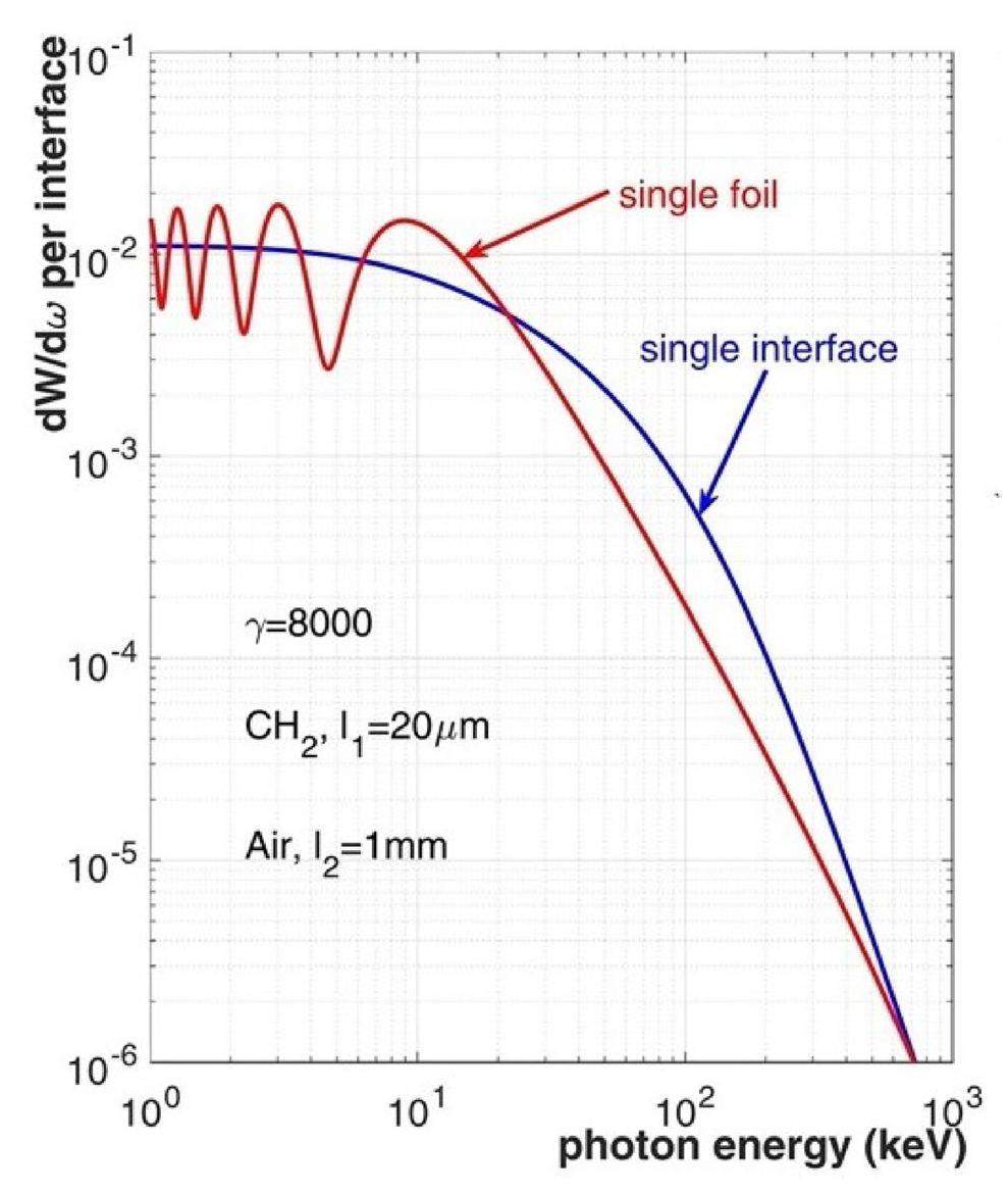
The TR of a single foil is coherent due to the existence of two interfaces, and the differential representation of its radiation intensity with the TR photon exit angle and frequency is given as:
For a radiator with N layers foil, the TR photon yield is a superposition of the yields of 2N interfaces, taking into account the self-absorption of TR photons by the radiator material, which is expressed as:
TR characteristics can be briefly summarized as a few points: (1) TR photon energy from the radiator exit mainly in the X-ray energy region; (2) TR photon yield of single interface is very low, with the same order of magnitude as α; (3) The N layers foil-stacked radiator has coherence, and its TR photon yield is about 2N times of the single interface; (4) The angle between the exit direction of the TR photon and the direction of motion of the incident charged particle is very small, and the most probable emission angle is θMPV≈1/γ; (5) Relativistic charged particles with same charge Z and same Lorentz factor γ have the same TR intensity, and their radiation yield is proportional to the square of the charge of the incident charged particle Z2, while is also proportional to the Lorentz factor γ.
Briefly Consideration For TRD Design
The radiators in TRD come in two types: regular and irregular. Regular radiators tend to yield higher levels of TR photons compared to irregular radiators of the same thickness. However, irregular radiators offer a more stable mechanical structure, making them easier to fabricate. Avakian [440] extensively researched the relationship between TR yield and radiator parameters. An efficient TRD requires a high TR photon yield, with the number of interface layers in the radiator (foil layers, denoted as N) being a primary influencing factor. Opting for a foil material with a higher plasma frequency can enhance TR photon yield but necessitates a balance between foil density and self-absorption issues.
The energy range of TR photons depends on both the material and thickness of the radiator. In multi-layer foil radiators, several coherent peaks are present within the TR spectrum [441]. In practical applications, the focus is typically on the most energetic peak within the coherent spectrum. TRDs are employed for particle identification and γ measurements, and their measurement range is determined by radiator parameters. The TR intensity varies with γ, resulting in threshold and saturation effects [404], expressed as
For detectors used to measure TR, the most prevalent ones currently are straw tubes [426] and MWPC [427]. Straw tubes are typically made from materials like polyimide or Mylar coated with aluminum, with diameters ranging from a few mm to several cm, often assembled in rows to form modules. MWPC are more suitable for large-area applications. The choice of working gas directly influences the detection efficiency of TR photons, where Xenon stands out as the optimal choice, although Argon has seen use in NUSEX and MACRO experiments. For measurements in higher energy ranges, considering new types of detectors becomes necessary, such as the Compton scattering TRD proposed by the ACCESS experiment [442].
The readout electronics vary based on different applications. A classic example is the difference between the readout electronics in the ALICE experiment’s TRD, which adopts a slow readout method, and those in the ATLAS experiment, which, due to high collision luminosity, requires a fast readout system. TRDs used for measuring TR emission angles require electronics with two-dimensional readout capabilities, such as those utilizing the Timepix3 chip-based readout for TRD [443].
ALICE TRD
The TRD in the ALICE experiment not only facilitates e/π discrimination but also enables track reconstruction [427]. Comprising 522 readout chambers, it encircles the central part of ALICE, dividing it into 18 sections. Each section consists of 6 layers, with 5 readout chambers per layer. These chambers comprise radiators and MWPCs. The radiators consist of polypropylene fibers and two layers of Rohacell foam HF71, totaling 4.7 cm. Each readout chamber is divided into a 3.0 cm drift region and a 0.7 cm amplification region. The working gas is Xe/CO2 (85%/15%), and its detector module is depicted in Fig. 95.
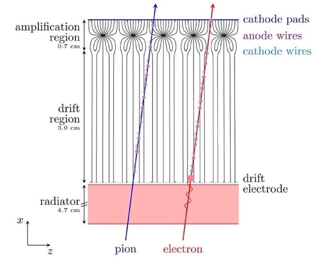
According to ionization signals, the ALICE TRD can reconstruct particle tracks with a position resolution of up to 700 µm. As depicted in Fig. 96, for particles with a momentum of 1 GeV/c and a 90% electron efficiency, employing the simplest algorithm, LQ1D, arrives a π rejection factor of 70. When incorporating the timing information of its signal, the rejection factor reaches 410.
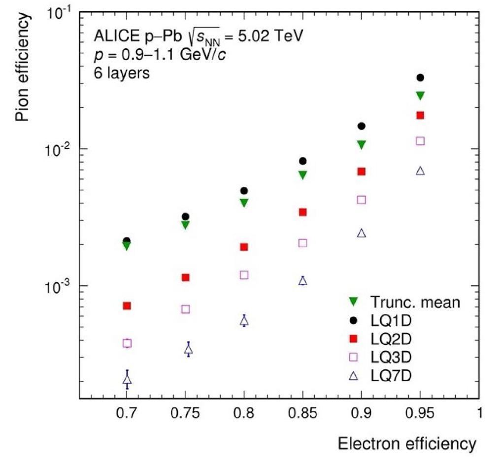
AMS-02 TRD
The particle identification capability of the TRD is closely linked to the intensity of the TR signals it detects. One effective method to enhance the TR signal strength involves increasing the number of modules within the TRD. The AMS-02 experiment [432, 444, 445] utilizes a 20-layered TRD, as depicted in the experimental setup shown in Fig 97. Each single TRD layer consists of 2.0 cm thick irregular radiators and straw tubes with a 0.6 cm diameter. The radiators contain fibers with a diameter of 10 µm, and the straw tubes, measuring 2 m in length, have walls comprised of two layers of aluminum-coated Kapton film, each 72 μm thick. The operating gas is a mixture of Xe/CO2 (80%/20%) at a pressure of 0.9 bar. Every 16 straw tubes constitute a module, illustrated in Fig. 98, resulting in a total of 5248 straw tubes across the 20 layers. Additionally, the intermediate 12 layers facilitate three-dimensional reconstruction of particle trajectories. To ensure gas stability during operations, a gas circulation system carrying 48 kg of Xenon and 5 kg of CO2 is deployed in orbit.
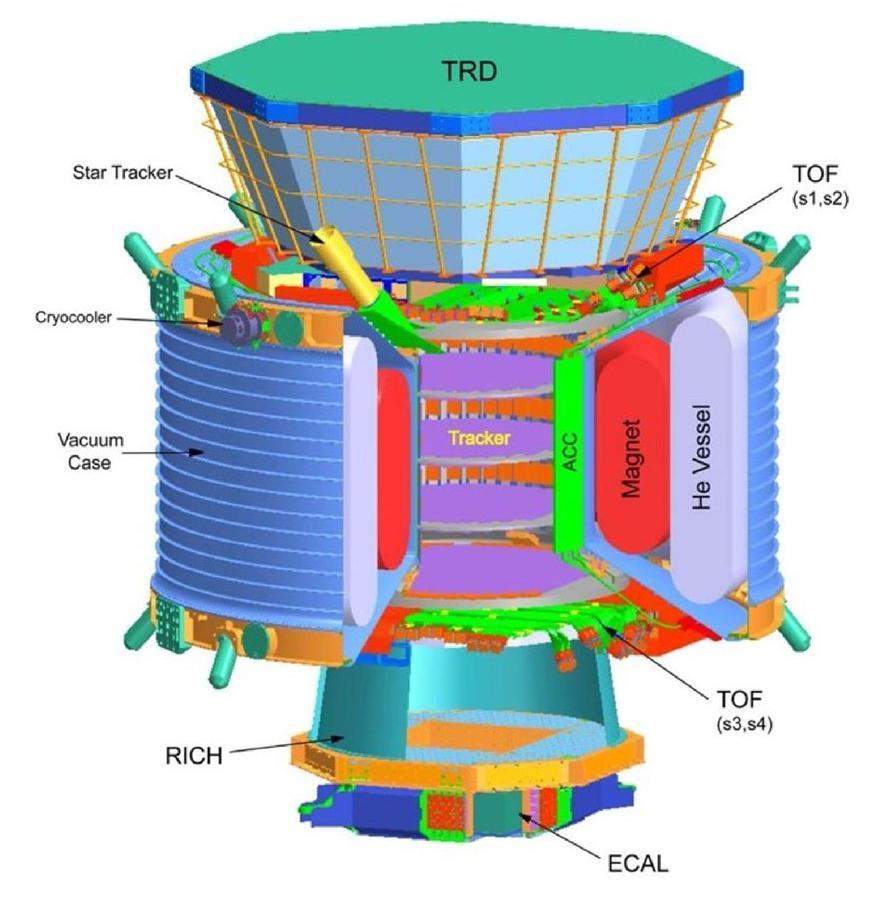
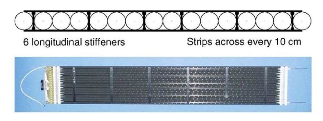
The probability density function is constructed using the maximum likelihood method for the deposition energies of electrons and protons, and the beam test and on-orbit results for TRD particle identification are shown in Fig. 99, for protons with a rejection factor higher than 103 at 90% electron efficiency.
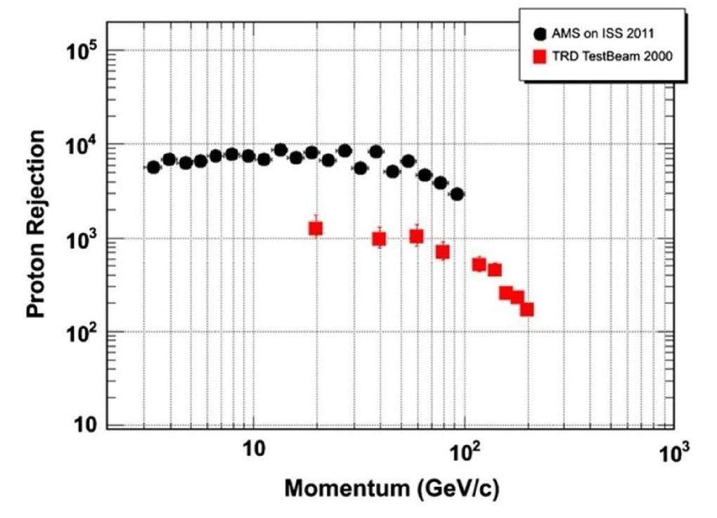
TRACER TRD
The TRACER experiment utilizes TRD as a cosmic ray energy measurement instrument for high-Z cosmic ray nuclei spectra [437]. The TR intensity is directly proportional to the square of the charged particle’s charge, resulting in better measurement resolution with higher charge values. The schematic diagram of TRACER, shown in Fig. 100, consists of four TRD layers, each comprising a radiator and rear-facing double-layered straw tubes. The first layer employs a thick-type radiator with an average fiber diameter of 17 μm and a thickness of 17.8 cm. The subsequent three layers are thin-type with fibers approximately 4.5 μm in diameter and each layer is 11.25 cm thick. This design advantageously allows high-energy TR photons produced in the first layer’s radiator to partially pass through the first TRD straw tubes and be detected by the subsequent three layers, exploiting this “feedthrough effect" to enhance the measured TR signal intensity. The straw tubes are made of aluminum-coated mylar foil, 2 cm in diameter and 200 cm in length, with a working gas mixture of Xenon and CH4. The initial two balloon flight tests (T99, LDB1) utilized Xe/CH4 (50%/50%) at a pressure of 0.5 bar, while the third flight test LDB2 employed Xe/CH4 (90%/10%) at a pressure of 1.0 bar. Additionally, a 3000 L gas circulation system was carried to ensure the stability of the working gas. During the LDB2 flight test, a resolution of 8% was achieved for cosmic ray iron nuclei at 1500 GeV/amu.
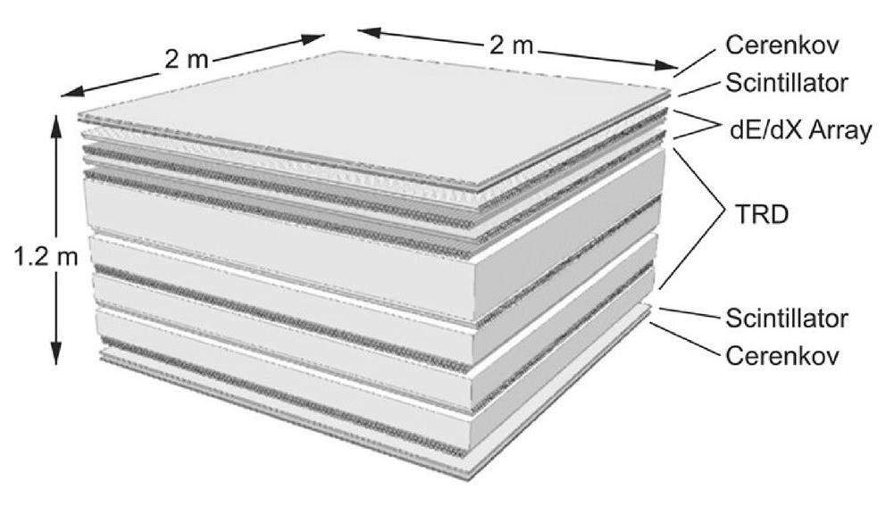
Newest Implementations Of TRDs
In recent years, there have been new applications and developments of TRDs. With the development of new chips for pixels, which made it possible to measure the fine structure of TR emission angles, and a silicon pixel-based TRD based on the TimePix3 chip [443] made fine measurements of the distribution of TR emission angles. In order to measure the distribution of TR emission angles, the TR photons with different exit directions must be separated in the detector. By adding helium tubes between the radiator and the pixel detector to increase the movement distance of the TR photons, the TR photons are able to be separated in the pixel detector, and the distribution of the TR photons with the angle is reconstructed by the cluster algorithm, a typical measurement result is shown in Fig. 101.
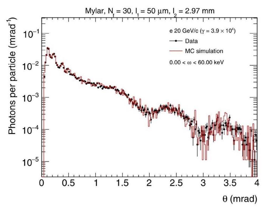
Besides the classic TRDs based on straw tubes and MWPC, in recent years, TRDs based on Thick Gas Electron Multiplier (THGEM) have been developed and applied [439, 446]. Using the THGEM as a replacement for the traditional anode wires for electron multiplication helps avoid issues related to wire aging. Figure 102 illustrates a side-on TRD based on a double-layers THGEM [439]. The radiator consists of 300 layers of stacked polypropylene foils with a thickness of 20 μm and 500 μm air gaps, providing an effective area of 5 cm × 5 cm. The detector comprises a TPC utilizing a double-layers THGEM for electron multiplication, operating with an Ar/CO2 (93%/7%) gas mixture at a pressure of 1 atmosphere and a gas thickness of 5.1 cm. The radiator is installed on the side of the TPC. This TRD prototype is designed for high-energy cosmic ray detection facility to calibrate cosmic ray energies in the TeV range. A typical TR spectrum from electronic beam tests of this TRD prototype is shown in Fig. 103.
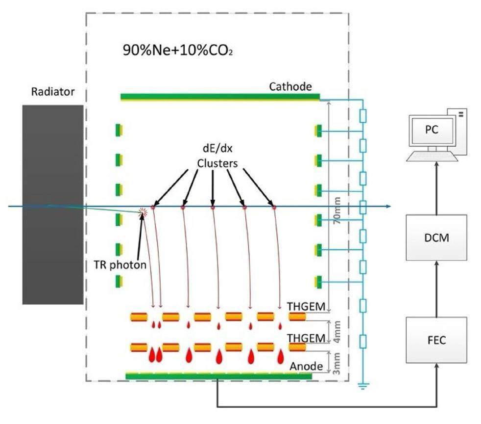
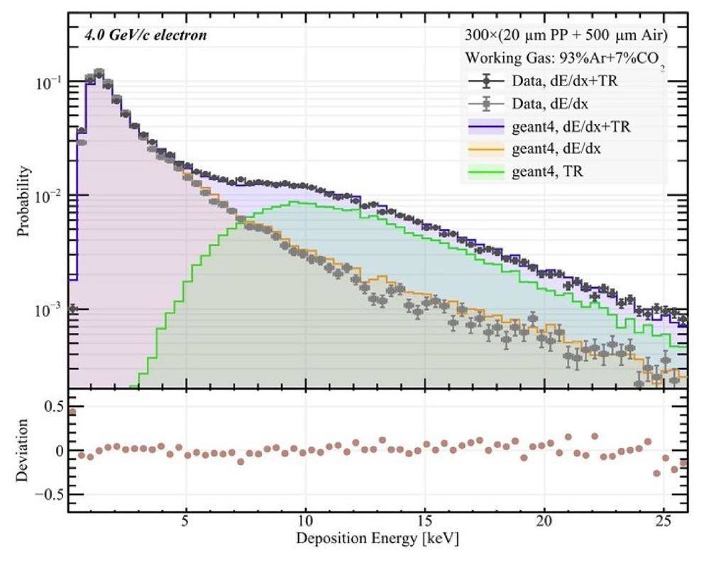
Readout Technology
Introduction
Readout system plays a pivotal role in physics experiments. As shown in Fig. 104, the readout system architecture mainly consists of the Front-End (FE) part, the Back-End (BE) part, and the Data Acquisition (DAQ) software. However, the scale of readout system varies significantly among various physics experiments.
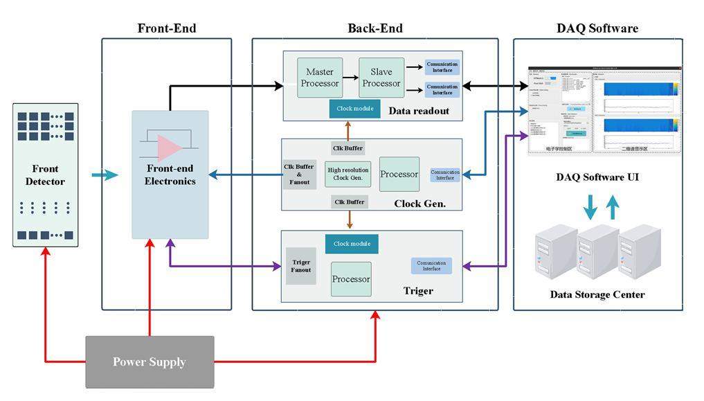
The electronics in the FE part handle the detector signal and extract the critical physical information. The BE part typically comprises the data readout blocks, the clock and synchronization blocks, and the trigger blocks. It provides high-bandwidth links for transmitting data and other signals and, in some cases, resources for online data processing algorithms. The DAQ software generally facilitates human-computer interaction to control the overall system and store the data.
The boost of modern physics experiments allows physicists to explore the universe but brings new challenges to data acquisition, in particular, higher radiation levels, higher channel density, significantly more data, and accurate measurement of the original detector signal. This chapter will discuss some state-of-the-art techniques in data acquisition to face these challenges in physics experiments.
Waveform Digitization
The waveform of the detectors’ output contains the most comprehensive and detailed physical information. The waveform area of the signal represents the energy deposited by the particles in the detector. The leading edge of the signal waveform carries the time information of the particle hitting the detector. Traditionally, energy measurement consists of a charge-sensitive amplifier, shaping circuit, and analog-to-digital converters (ADCs). Time measurement consists of fast amplifiers, discriminators, and time-to-digital converters (TDCs). Waveform digitization technology directly sample and digitize the waveform of the detector output signal at high speed. The traditional charge integration and shaping are no longer carried out, and the particle’s energy and time information is obtained digitally. According to Shannon’s law of sampling, as long as the sampling rate is high enough, the original pulse waveform can be reconstructed without distortion. The waveform digitization technology can conveniently obtain time and energy information simultaneously, eliminates the pile-up effect caused by the traditional charge integral amplification, and has a short dead time. Hence, it suits physical experiments with high luminosity and event rate. In addition, the waveform digitization technology allows physicists to employ possible digital processing methods. One common way to realize waveform digitization is to use fast-commercial ADCs. Later, a new technique uses the switching capacitor array (SCA) ASIC to achieve ultra-high-speed analog sampling and digitize the waveforms using ADC inside or outside the ASIC. All in all, increasing the sampling rate is a core of the waveform digitization technology.
As the fastest type of ADC, the Flash ADC plays a primary role in waveform digitization. An N-bit flash ADC consists of 2 N resistors and 2N-1 comparators arranged as in Fig. 105. Each comparator has a reference voltage from the resistor string, which is 1 LSB higher than the one below it in the chain.
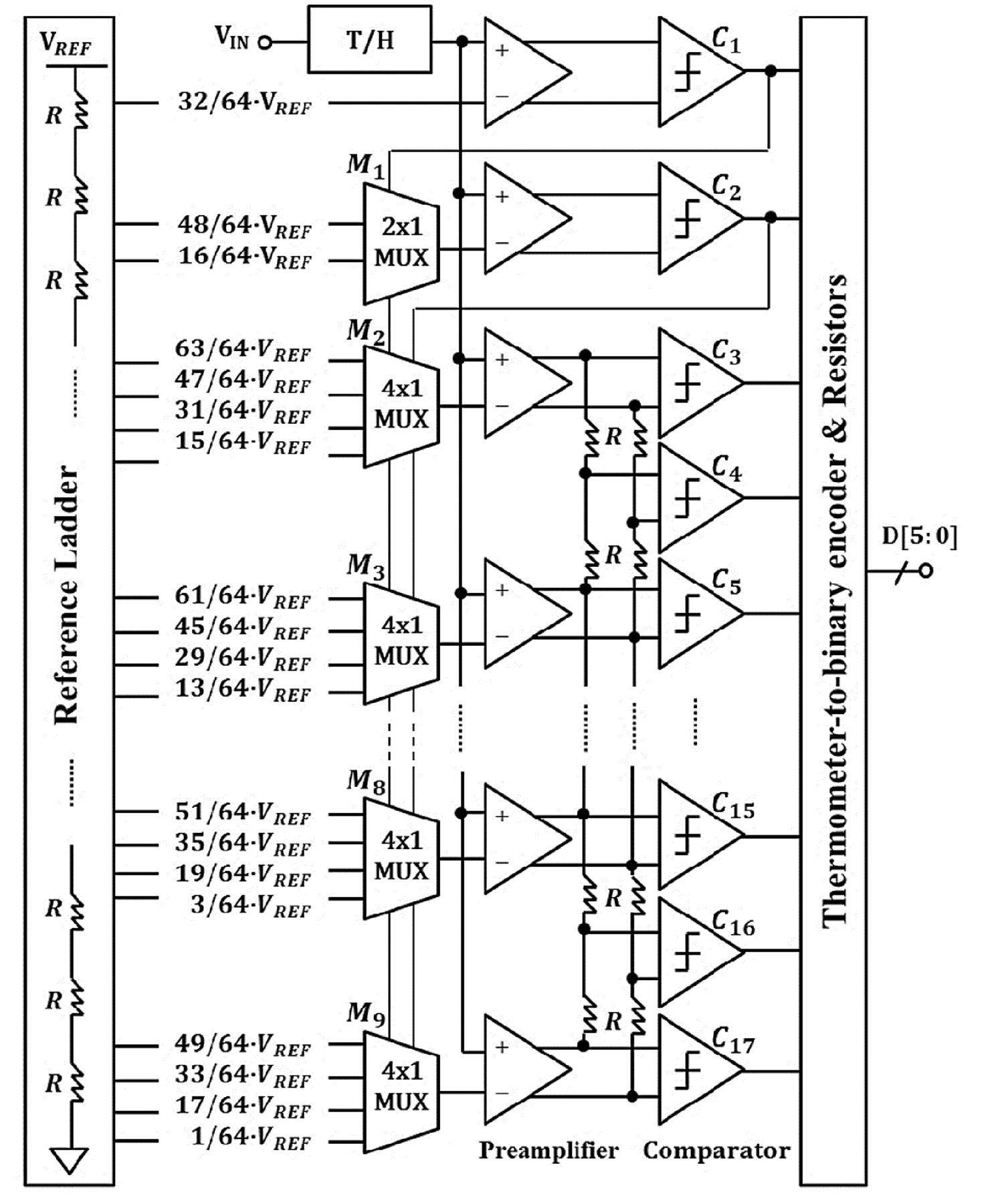
As early as 1985, European scientists used 100 MSPS flash ADCs [449] for the signal readout of the vertex detector in the UA2 experiment at CERN. A typical example application is the MAGIC telescope [450]. The analog signals from the detector are continuously digitized by 8-bit 300 MHz Flash ADCs. This system has been working in Magic experiments until January 2007. Since then, the readout system has been upgraded with 2 GHz 10-bit ADCs [451, 452]. Waveform digitization is also included in the readout electronics for the Large High Altitude Air Shower Observatory (LHAASO) KM2A [452]. The output signal from the KM2A detector is passed through a shaping circuit with a time constant of 10 ns and continuously digitized by a 500 MHz 12-bit flash ADC with 9.3 effective bits. Commercial higher-power stand-alone flash ADCs are available with sampling rates over 1 GHz. However, the significant disadvantages are higher power dissipation, lower channel density, higher cost, and the generally limited resolution of 6 - 10 bits. The pipeline ADC is a popular structure that offers high speed and high resolution, with moderate power dissipation and a small die size. The External-target Experiment (CEE) at the HIRFL-CSR will be a large-scale GeV nuclear physics experiment independently developed in China. The Zero-degree calorimeter [453] uses is a 16-channel, 14-bit pipeline ADC (AD9249) [454] with a sampling rate of 65 MHz to realize waveform digitization. For the MAPS in heavy-ion physics, a regional 12-bit 40-Msps pipeline ADC has been designed to convert the analog signals from the pixels into digital data [455]. Time-interleaved ADC (TI-ADC) is a multi-channel data-parallel acquisition technique that breaks high-speed and high-accuracy bottlenecks. However, calibrating the various mismatch factors (gain, clock phase/skew, offset) is essential. Common correction algorithms are within FPGAs: gain and offset errors are corrected by adders and multipliers, and the time-skew error is corrected based on a fully parallel correction method [456]. Another new approach to calibration is using an additive-neural network-based digital calibration algorithm for nonlinear amplitude and phase distortion [457, 458].
Over the last decade or so, due to the development of the Switched Capacitor Array (SCA) has been an excellent solution for waveform digitization because of its low power consumption and high channel density at affordable costs compared to high-speed ADCs. Figure 106 is the schematic of a SCA circuit. The SCA, controlled by a high-speed domino ring chain, samples, and stores the input voltage signal. The fast SCA ASIC typically combines with low-speed ADCs for analog-to-digital conversion. Various SCA ASICs have been designed for physics experiments, and the sampling rate ranges from GHz to MHz. The GHz sampling SCA chips are mainly used for fast scintillation or Cherenkov light detectors. The DRS4 [459] chip from the Paul Scherrer Institute is a radiation-hard SCA fabricated in a 250 nm process. The DRS4 has nine differential input channels, each with 1024 sampling cells. This ASIC can provide up to 5 GHz sampling speed, and the signal-to-noise ratio allows a resolution equivalent to more than 11 bits, and 4 ps timing resolution. The DRS4 has been used in MAGIC-II [460], PADME [461], CTA [462], etc. The PSEC4 [305] from LAPPD Collaboration is also representing GHz SCA ASIC. It has six input channels, each with 256 storage capacitors. The sampling rate can vary from 4 GHz up to 15 GHz. The PSEC4 has been used in a water-based optical time-projection chamber (OTPC) [463], large area picosecond photodetectors (LAPPDTM) [464], etc. In addition, the MHz sampling SCA chips also play an essential role in semiconductor and gas detectors. These SCA chips usually integrate the front-end circuit and the capacitor array. The representing ones are the AGET [215] chip from N. Usher and AT-TPC collaboration and the GERO [465] chip from Tsinghua University. The AGET has 64 channels, and each channel integrates mainly a charge-sensitive amplifier (CSA), an analog filter, a discriminator, and 512 storage capacitors. The sampling frequency of the AGET can change from 1 MHz to 100 MHz. The AGET has been used in many time projection chambers (TPCs), such as active target and time projection chamber [217] (ACTAR TPC), PandaX-III TPC [466], and texas active target [467] (TexAT). The GERO chip, fabricated in a 180 nm CMOS process, has 16 channels, each with a storage array with a 1024-cell depth and 32 Wilkinson ADCs. The sampling speed can vary from 1 MHz to 100 MHz. The GERO chip is a good candidate for micro-pattern gas detectors [465]. Similar MHz SCA ASICs are the BEETLE chip for LHCb [468], the DTMROC and HAMAC chips for LHC ATLAS [469], and the CryoSCA chip for HPGe detectors [470].
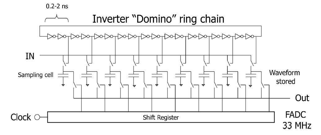
All in all, waveform digitization is an excellent candidate to fulfill the physicist’s dream of original signals from the detectors, and many do-of-experiments have been studied. This technology has great potential to change the architecture of data acquisition schemes for future physics experiments and a wide range of related applications. However, this technology still needs technology development to replace the traditional one.
High-speed Radiation-tolerant Data Transmission Link
The data transmission link is an essential component of the data acquisition system. With the development of physics experiments, higher data scales and radiation environments have put higher demands on data transmission links, requiring the development of higher transmission rates and radiation tolerance. In addition, high-density detectors also require lower power consumption in data transmission links, which has become one of the future research directions. A wireline transmission link generally consists of Serializer/de-serializer (SERDES) and optical modules. The SerDes serializes and deserializes the data for high-speed serial transmission, avoiding the data skew issue. Optical modules convert electrical signals into optical signals for transmitting data over an optical fiber for long-distance transmission. In addition, several techniques can improve transmission speed, distance, and stability, such as clock recovery, equalizer, and line coding. Clock and data recovery circuits (CDR) recover clocks from the received data without transmitting clocks, avoiding the skew between data and clock. Equalizers compensate for signal attenuation during transmission. Line coding enhances the anti-interference ability of transmission to increase reliability.
The GigaBit Transceiver (GBT) from Large Hadron Collider (LHC) is the most typical radiation-tolerant SerDes transceiver [471, 472]. The GBT is implemented in a 130 nm technology and can achieve an uplink and a downlink at the data rate of 4.8 Gbps. As shown in Fig. 107, the GBT converts the parallel input into serial output and the serial input into parallel output. The triple module redundancy technique can improve radiation tolerance. However, it would impose a speed penalty on the circuit, preventing the high-speed implementation of transceivers. To improve radiation tolerance without reducing the circuit speed, the GBT didn’t apply any redundancy techniques on the data path between the input of the serializer and the output of the de-serializer but instead transmitted the data with Forward Error Correction (FEC) code. The FEC technique is an Error Control Coding (ECC), which encodes data at the input of the serializer and decodes data at the output of the de-serializer. Bit errors can be detected and corrected during decoding, thus reducing the bit error rate.
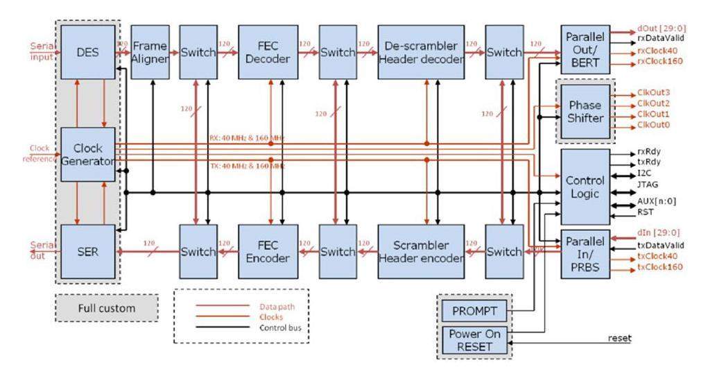
To withstand the radiation levels and the data bandwidth requirements of the phase-2 High Luminosity LHC (HL-LHC) detector upgrades, a low-power GigaBit Transceiver (lpGBT) in 65 nm technology was proposed [473]. With a radiation tolerance of 200 Mrad, the lpGBT shown in Fig. 108 achieves an uplink data rate of 5.12/10.24 Gbps and a downlink data rate of 2.56 Gbps. Except for the speed and radiation tolerance request, low power is also the aim of lpGBT. By optimizing the architecture, such as using only one PLL to serve all, lowering the supply voltage, and so on, the lpGBT reduces the power consumption.
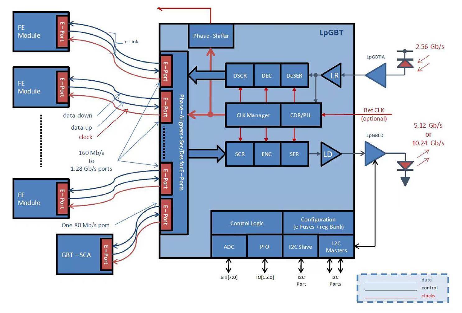
Except for the GBT and lpGBT, several transceivers have been developed for physics experiments, such as the GBCR1/2 for the ATLAS Inner Tracker Pixel Detector [474], the LOCx2 fro the ATLAS Liquid Argon Calorimeter [475], the NICA_GBTx [476] for the NICA Inner Tracker, the Hi’GBT [477, 478] series for HIRFL and HIAF and so on.
The optical module used with the GBT at LHC is a Versatile link transceiver (VTRx) [479], operating at rates up to 4.8 Gbps. It can support a transmission length of 150 meters, featuring radiation-resistant, magnetic field tolerant, low-power, and low-mass front-end components. The link supports single-mode (SM) operation with a center wavelength of 1310 nm and multi-mode (MM) operation with a center wavelength of 850 nm. In addition, a Versatile link+ transceiver (VTRx+) [480] shown in Fig. 109 is used in tandem with the lpGBT, operating at rates up to 5.12/10.24 Gbps in the uplink and 2.56 Gbps rates in the downlink.
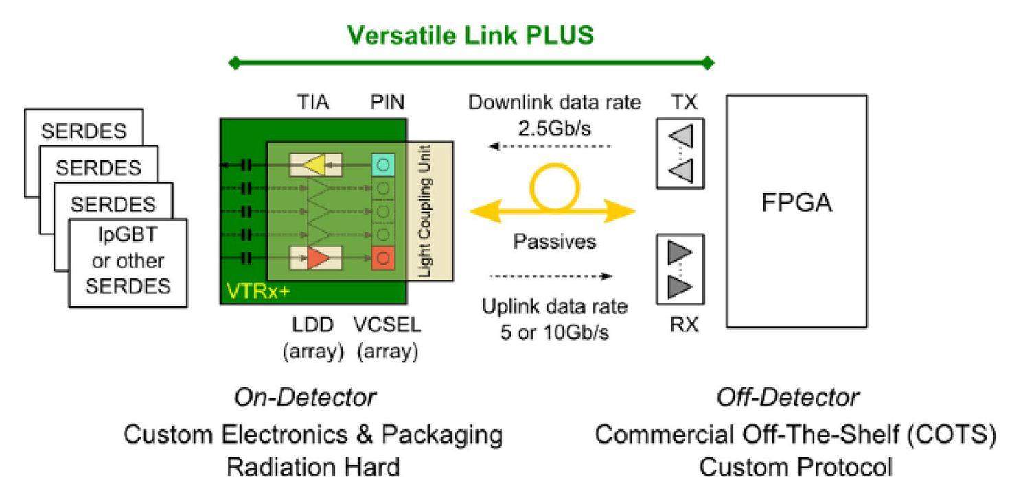
Except for the VTRx and the VTRx+, several optical modules used in physics experiments have been developed, such as a 5 Gbps compact parallel optical engine proposed by the Ohio State University [481], a dual-channel VCSEL driver LOCld-130 designed in 130 nm CMOS technology [482], a 20 Gbps PAM4 VCSEL driving ASIC for detector front-end readout[483], a 14 Gbps optical transceiver ASIC (LDLA14) fabricated in a 55 nm CMOS technology for NICA [484], and so on.
Trigger-less Readout System
Many contemporary physics experiments employ multistage readout and trigger architectures to handle the vast data throughput generated by the detector elements. Conventional readout systems are a compromise between the goal of maximizing experimental data acquisition and the technical limitations of online data processing and storage. For physics experiments with high event rates, high channel counts, and front-end caching constraints, the trigger-less readout system is an excellent data acquisition solution. The term "trigger-less" does not imply the absence of a trigger but rather that there is no global hardware trigger signal. Generally speaking, the front-end electronics adopts the self-triggering approach, and back-end electronics employs the software-triggering or trigger-less method when designing a trigger-less readout system. Over the past few years, various new readout architectures have been developed with trigger-less to increase the fraction of data collected and stored for offline analysis. Some noteworthy examples include trigger-less readout systems for experiments or detectors such as PANDA [485-489], Mu3e [490-492], CBM [493-495], and more.
In the PANDA experiment, all detector channels operate in self-triggering mode, and the synchronized data from all detectors is processed online to find the critical physical quantities [485]. Figure 110 takes the readout architecture of the PANDA Electromagnetic Calorimeter (PANDA-EMC) as an example. The detector signal is read out by a large area avalanche photodiode (LAAPD), which is then amplified using a preamplifier. The amplified signal is continuously digitized by sampling ADCs (SADC) within the digitizer module. The digitized data is processed in real-time by the field-programmable-gate-array (FPGA) with feature extraction algorithms, including dynamic base-line compensation, hit detection, and hit information extraction [488, 489], to analyze the data and extract relevant information, e.g., energy and time of the hit [485]. These processed and refined data are transmitted through optical links to a data concentrator module (DCON), a nexus for several digitizer connections [485]. Then, the DCON module carries out online pile-up recovery, energy calibration, and event pre-building tasks[485-487]. The data then passes to the FPGA-based Compute Node for final event construction and selection [485]. Additionally, the DCON module takes in a clock signal and synchronization commands from the Time-Distribution module, redistributing this information to digitizer boards with consistent latency since the digitizers require extremely strict synchronization on timing [485].
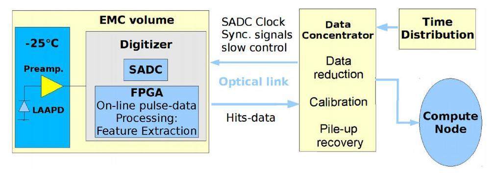
Hence, there is no global trigger signal in the PANDA-EMC readout system, which uses a self-triggering FE to acquire data and a high-bandwidth DCON as a BE to consolidate and pre-processed data from several digitizers. This approach ensures efficient data collection and processing, and the PANDA experiment is expected to benefit from trigger-less readout systems.
As shown in Fig. 111, the readout system for the Mu3e experiment has four stages. The first and second stages constitute the FE part, the third stage makes the BE part, and the fourth stage contains the DAQ software. The first stage contains 3122 ASICs [491], which include 2844 MuPix [496, 497] sensors and 278 MuTRiGs [498]. The second stage consists of 114 front-end boards, which receive the data from the first stage via LVDS links with a speed up to 1.25 Gbps. The initially unpacked data are grouped into the detector-specific record type by the second stage and then transmitted to the third stage through up to two 6.25 Gbps optical links [490]. The third stage consists of four switchboards, each fitted with a high-performance FPGA designed to execute time alignment of the hit data, ensuring synchronous processing and integration of the information [490, 491]. The Mu3e filter farm, functioning as the fourth stage, uses sixteen 10 Gbps optical links from switching boards that connect to a daisy-chained network of twelve PCs, each endowed with a Graphics Processing Unit (GPU) and a fast FPGA card [490]. The FPGA card integrated into the PC consistently receives hit data, ensures time alignment, and buffers it in DDR4 memory on the FPGA card while also transcoding hit coordinates into the global detector coordinate system before populating the cache memory of the PC. Upon DDR4 memory saturation, the system autonomously redirects the data to the subsequent PC in the daisy chain, thus implementing a rudimentary load-balancing schema that circumvents data congestion by distributing the data stream among multiple units. The hit data in the cache memory of the PC is transferred to the GPU, which is responsible for trajectory reconstruction and selective filtering [491]. Upon completion of these processes, the post-processed datasets are transmitted to a data collection server named Maximum Integrated Data Acquisition System (MIDAS) [490] through the Ethernet connection for subsequent storage [490, 491]. Notably, the Mu3e readout system differs from the PANDA-EMC readout system in two ways. First, it utilizes a powerful GPU in data processing. Second, it uses large-capacity data storage. These advancements improve the efficiency of the Mu3e DAQ system, promoting the versatility of trigger-less systems in accommodating the demands of different experimental setups.
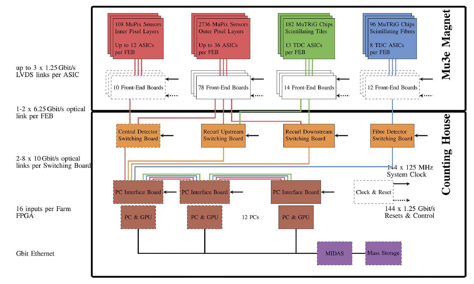
The CBM experiment is another example of a recent trigger-less readout system design. Take the Silicon Tracking Source (STS) as an example, which poses a vital challenge to the data transmission in the CBM experiment. Like the Mu3e experiment, the STS readout system also uses a four-layer structure, as shown in Fig. 112. The FE part of the STS subsystem, consisting of 1800 front-end boards (FEBs), operates in a self-triggering mode as the primary layer. At the same time, the BE part of the STS subsystem, including ∼ 600 Readout Boards (ROBs) as the second layer and roughly 80 Common Readout Interface cards (CRIs) as the tertiary layer, employs a trigger-less streaming readout design method. The final layer consists of a central Timing and Fast Control system (TFC), orchestrating the synchronization and control across the subsystem [494].
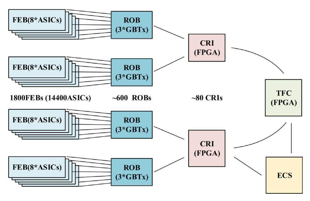
The challenge of high data bandwidth in the STS readout system has been addressed with a throttling mechanism [494], which is triggered when the data transmission links of the FE part are getting saturated. Fig. 113 shows the hardware function of the throttling mechanism. The throttling logic, implemented in the FE ASIC and firmware, sends an alert to the controller when the number of near-full channels exceeds a programmable threshold. Two throttling strategies, "Stop" and "Clear," have been studied and implemented [494]. Under the "stop" strategy, once the internal channel FIFOs of the ASIC get full, the system will stop accepting any more hit data and wait until the FIFO has been completely read out before it starts to retake new hits. On the other hand, the "Clear" strategy clears the channel FIFOs in ASIC through a resetting process and then quickly re-enables data taken by releasing the reset [494]. Experimental study shows the "Stop" strategy can read more valid data than the "Clear" strategy but has a more significant time penalty. Thus, selecting a throttling method becomes a trade-off between data completeness and time efficiency [494]. The STS readout system of the CBM experiment illustrates how trigger-less systems can be adapted to deal with high data volumes, further underlining their versatility and robustness in modern physics experiments.
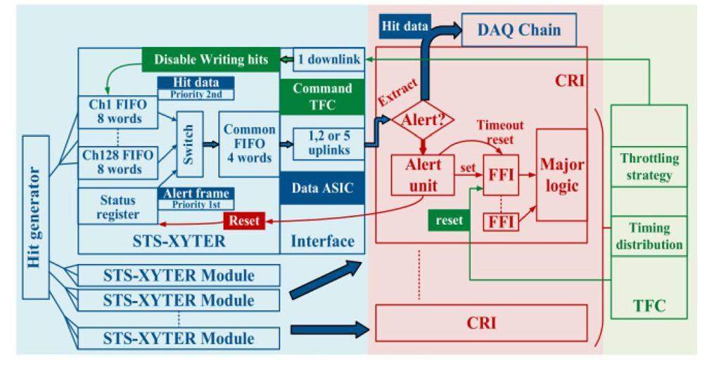
Generally, the FE part of a trigger-less readout system often operates in a self-triggering mode for data readout. It includes a digitization module to digitize the detector signal. The BE part is designed with substantial bandwidth capabilities and typically works in trigger-less or software-triggering modes. Additional methods are implemented to decrease the data volume at the FE when necessary. Interestingly, it’s also possible for the BE data readout process to be intervened or manipulated with software to further reduce the amount of data, as demonstrated in some studies. The trigger-less readout system has excellent flexibility and adaptability in handling high data volumes, making it a fancy solution for modern physics experiments.
Artificial Intelligence in on-line data processing
Machine Learning (ML), the first generation of Artificial Intelligence (AI), allows a system to learn and improve from experience without being explicitly programmed automatically. Arthur Samuel from IBM invented the first-ever machine learning program. ML has two types: supervised learning and unsupervised learning. Supervised learning trains the model to find the relationship between the labelled input and output. So, the model can predict new output with new input. The accuracy of supervised learning can be measured directly. Unsupervised learning trains the model to find the hidden structure from "unlabeled" data. It is not looking for something specific but for structure or anomaly patterns. Evaluation of unsupervised learning usually in indirect or qualitative methods. ML, especially supervised learning, has significantly benefited physics data analysis for decades as a powerful tool for data volume reduction and interesting event selection from the vast and complex data from modern physics experiments. Supervised ML models can be generally categorized into classification and regression models. The former classifies input data into two or more classes. The latter predicts continuous valued output based on the input. Later, the advent of the Neural Network [499] and deep learning [500] provides more powerful tools to analyze more complex and higher dimensional data. ML methods achieved wide success in particle physics research [501], with early applications to high-level analysis in the 2000s, followed by event identification and reconstruction in the 2010s [502].
Figure 114 shows the data reduction methods (triggering scheme) of LHC, which usually consists of two levels of triggers. Level 1 (LV1) typically implements with FPGA-based hardware, receiving several Tb/s data, generating trigger decisions in the scale of µs. The LV1 reduces the data volume to several Gb/s based on identifying local objects that represent candidates for identification [503]. The High-Level Trigger (HLT), using farms of CPUs or GPUs, makes decisions on the scale of 100 ms for a particular event based on complete event information from all the detectors, close to offline algorithms [503]. The HLT reduces the data from several Gb/s to several Mb/s. Increasing detector channels and event rate boosts the data volume, thus posing a challenge to the process capability of the trigger scheme. Hence, several recent research studies have applied AI-based approaches (machine learning, neural network, deep learning, etc.) to online data processing in detectors front-end ASICs, LV1, and HLT.
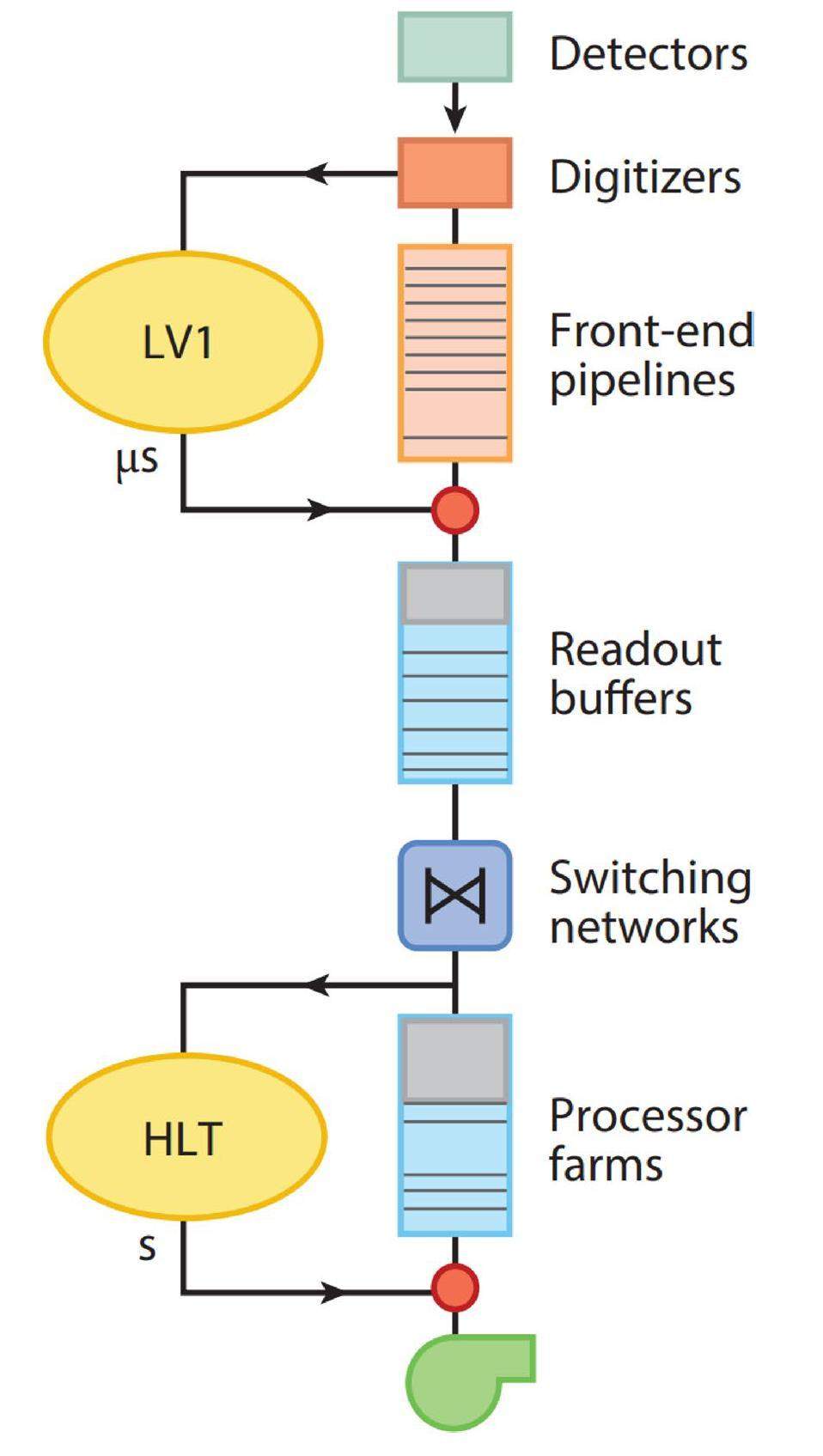
Data compression (trigger) in the front-end achieved many successes historically with zero-suppression, threshold-based selection, sorting or summing of data, etc, either on front-end AISCs, avoiding moving vast data from the detector to the readout electronics. The rapid development of the microelectronic industry drives the implementation of on-chip AI algorithms for detector signals, which are expected to extract information more efficiently [504]. implements an autoencoder with a neural network (NN) with programmable weight for data compression in the high-granularity endcap calorimeter (HGCAL) [505] of LHC CMS. Figure 115 shows this autoencoder maps the hexagonal sensor shape to a more typical Cartesian presentation for simpler training and implementation. Each inference consumes only 2.4 nJ, consists of 800k gates, occupies a total area of 3.6 mm2, and withstands a radiation load of up to 200 Mrad. [506] proposed the CMOS pixel sensor with an on-chip Artificial Neural Network (ANN) for the vertex detector of the International Linear Collider Collider (ILC). It is used to tag and remove clusters generated by charged particles from the beam background. [507] and [508] reported clustering algorithms based on column-level ADC and pixel-level ADC architecture, respectively. Clustering is the first step of preprocessing modules for artificial neural networks, which is used to select clusters from frames of raw data. Occupied surface and power consumption of corresponding ASIC design were presented. [509] proposed compact on-chip operators for cluster feature extraction, designed for CPS with on-chip ANN and reported corresponding performance. The operators are used to extract features related to the angle of incidence and fed into the ANN module. [510] designs a fast-stop centroid finder for MAPS to calculate the geometric centroid of the energy deposition region. In addition, column-parallel ADCs have also been developed for MAPS in [511, 512] for on-chip data processing. [513] and [514] present the PulseDL AISCs, a system-on-chip for extracting time and energy from the scintillator detector pulses with deep learning. The PulseDL can process one-dimensional pulse signals for classification or regression tasks. The PulseDL II incorporates a RISC CPU into the system structure for better functional flexibility and integrity. The most significant development direction of AI in the detector front-end is to optimize the algorithm network parameters to ensure the accuracy and efficiency of data processing within the extreme area and power consumption limitations.
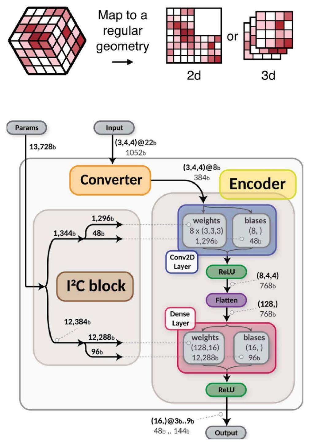
FPGA-based trigger systems can provide extremely low latency. This unique feature makes it a hot research point for particle physics. FPGA can be programmed with either Hardware Description Languages (HDL) or High-Level Synthesis (HLS). The hls4ml is a powerful tool that can translate machine learning tools into HLS code for implementation on an FPGA. Figure 116 shows the general working flow of the hls4ml package, where the red part is the usual working flow to build a neural network, and the blue part explains how the hls4ml works. [515] uses the hls4ml package to realize a fully-connected three-hidden-layer network in a Xilinx Kintex Ultrascale FPGA. This neural network is trained to identify jets originating from a light quark, gluon, W boson, Z boson, or top quark. The latency of the design is approximately 75 to 150 ns. Later, [516] studies how to use hls4m to reduce resource utilization with pruning and quantization-aware training without loss in model accuracy. It presents that the resource consumption can be reduced by 97% with zero loss on model accuracy and by 99% with a 6% accuracy loss. [517] reports a resource-efficient FPGA-based neural network regression model for ATLAS hardware muon trigger system, which achieves a simulated network latency and dead-time of 122 and 25 ns, respectively. [517, 518] proposed an FPGA-based L1 trigger system to perform similarly to the vertex fitting trigger but with fewer logic resources. Trigger decisions are created by a multilayer perceptron (MLP) model to distinguish the signal events from noise events and achieve an efficiency of higher than 99%, with a latency of ∼ 128 ns. As the beam in physics experiments gets more powerful, detectors will generate too much data, and the FPGA-based trigger system becomes more vital. The CMS also develops an FPGA-based tracking Level-1 trigger using the tracklet algorithm.
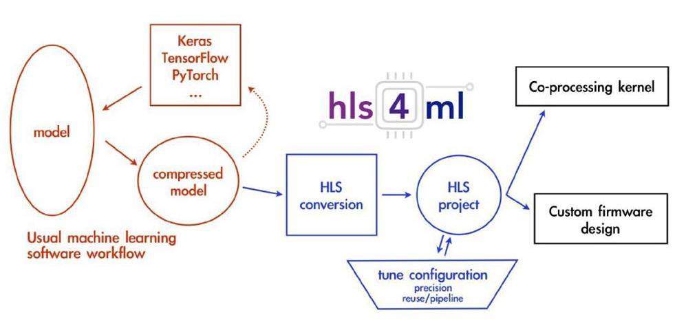
HLT implemented with state-of-the-art GPUs can provide more cost-effective parallel computation resources to realize online event selection. Numerous physics experiments have used GPUs in real-time data analysis, such as the RICH ring pattern reconstruction in NA62, the track reconstruction of the TPC track in ALICE, the decoding of raw data, clustering, vertex reconstruction, and muon identification in LHCb, etc. AI algorithms are expected to improve HLT’s performance. In [519], a residual convolutional neural network with four residual blocks in a binary classification scheme has been chosen for the software trigger of the PANDA experiment, which improves the efficiency gain with a factor of 2 while keeping the background reduction factor of 1/1000. In [520], The CLAS12 Electron trigger uses convolutional neural networks to select events based on the information from detectors. It achieves a 99.5% electron identification efficiency while reducing the volume of recorded data by 65%. [520] studies the cluster locating algorithms for the data from silicon pixels at HIRFL and HIAF. One-stage and two-stage detection algorithms (Fig. 117) have been constructed with Swin Transformer and ConvNext as the backbones. The cluster-locating algorithm based on deep learning presents nearly the same detection efficiency as the traditional Selective Search approach, improving the speed by one order. In addition, no fake triggers were observed in the test. A cheerful study in [520] demonstrates that deep learning algorithms optimized with available libraries are perfectly compatible with the operation constraints of a typical HLT environment. This study confirms that there is no technical challenge in deploying deep learning algorithms in the ATLAS and CMS HLT farms in the near future.
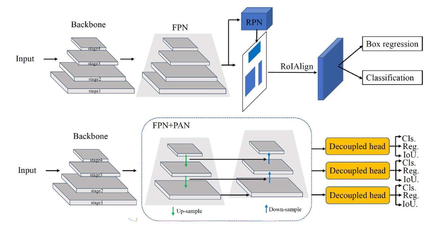
Conclusion and Outlook
Nuclear detecting techniques and nuclear electronics are the foundation of particle physics, nuclear physics, particle astrophysics, and other disciplines. In addition, nuclear detectors are increasingly used in fields such as nuclear power generation, life sciences, environmental sciences, space and plasma research, radiography, earth sciences, and biomedical sciences. Therefore, the study of nuclear radiation detection not only occupies a pivotal position in the scientific field, but also plays a vital role in the national economy, national security and defense construction, nuclear medicine, nuclear energy, and so on.
The main development trends of nuclear radiation detectors are: research on the detectors can simultaneously measure various information such as the position, energy, and time of the incident particles; developing detectors with higher granularity, better energy resolution, better time resolution, and higher detection efficiency; utilizing artificial intelligence to enhance the utilization of the information provided by the detector for analysis and processing; seeking new detection materials and detection mechanisms.
In the past, due to the impact of the market economy, the development of nuclear detection technology and nuclear electronics was affected in China. However, with the rapid growth of the national economy in recent years, the great demand for technology and talents in related application fields, and the entry of a large number of foreign commercial products, the development of nuclear detection technology and nuclear electronics has attracted much attention. Guided by national needs, China’s scientific researchers have completed the design and construction of several significant scientific research facilities, participated in and began to lead the development of international large-scale detectors, promoted technology transfer to industry, and served the national economy and national security.
An electrical method of counting the number of α-particles from radio-active substances
. Proc. R. Soc. Lond. Ser. A Contain. Pap. Math. Phys. Charact. 81(546), 141-161 (1908). https://doi.org/10.1098/rspa.1908.0065Early history of the scintillation counter
. Science 122(3157), 17-18 (1955). https://doi.org/10.1126/science.122.3157.17The scintillation counter
, in: Advances in Electronics and Electron Physics, vol. 4 (An inversion decomposition test based on Monte Carlo response matrix on the γ-ray spectra from nai (tl) scintillation detector
. Nucl. Sci. Tech. 27(4), 101 (2016). https://doi.org/10.1007/s41365-016-0104-8Semiconductor micropattern pixel detectors: a review of the beginnings
. Nucl. Instrum. Methods Phys. Res. Sect. A 465(1), 1-26 (2001). https://doi.org/10.1103/PhysRevLett.102.181101Single photon detection with semiconductor pixel arrays for medical imaging applications
, Ph.D. thesis,Ccd developments for particle colliders
. Nucl. Instrum. Methods Phys. Res. Sect. A 565(1), 157-164 (2006). https://doi.org/10.1016/j.nima.2006.05.061Skipper-ccds: current applications and future
. Nucl. Instrum. Methods Phys. Res. Sect. A 1046, 167681 (2023). https://doi.org/10.1016/j.nima.2022.167681Science with the 2.5-meter wide field survey telescope (wfst)
. Sci. China Phys. Mech. Astron. 66(10), 109512 (2023). https://doi.org/10.1007/s11433-023-2197-5Design of ccd test platform of scientific imaging for wide field survey telescope
. J. Astron. Telesc. Instrum. Syst. 8(1), 016005 (2022). https://doi.org/10.1117/1.JATIS.8.1.0160053d microstructures of nuclear graphite: Ig-110, nbg-18 and ng-ct-10
. Nucl. Sci. Tech. 27(3), 66 (2016). https://doi.org/10.1007/s41365-016-0071-0Characterization of silicon microstrip sensors for space astronomy
. Nucl. Sci. Tech. 31(10), 97 (2020). https://doi.org/10.1007/s41365-020-00811-9Compact 16-channel integrated charge-sensitive preamplifier module for silicon strip detectors
. Nucl. Sci. Tech. 31(5), 48 (2020). https://doi.org/10.1007/s41365-020-00755-0The dark matter particle explorer (dampe) and the very large area gamma-ray space telescope (vlast)
.Radiation damage experience at cdf with svx’
. Nucl. Instrum. Methods Phys. Res. Sect. A 383(1), 155-158 (1996). https://doi.org/10.1016/S0168-9002(96)00621-3Svx’, the new cdf silicon vertex detector
. Nucl. Instrum. Methods Phys. Res. Sect. A 360(1–2), 137-140 (1995). https://doi.org/10.1016/0168-9002(95)00087-9The cdf silicon vertex detector
. Nucl. Instrum. Methods Phys. Res. Sect. A 342(1), 240-250 (1994). https://doi.org/10.1016/0168-9002(94)91434-6Characterization of silicon modules and sensors for the ATLAS inner tracker strip detector
. Ph.D. thesis,Studies on silicon strip detectors for the CMS experiment
. Ph.D. thesis,Silicon tracking detectors in high-energy physics
. Nucl. Instrum. Methods Phys. Res. Sect. A 666, 25-46 (2012). https://doi.org/10.1016/j.nima.2011.11.005A gas-filled recoil separator, shans
. Nucl. Instrum. Methods Phys. Res. Sect. B 317, 315-318 (2013). https://doi.org/10.1016/j.nimb.2013.05.062MUST: a silicon strip detector array for radioactive beam experiments
. Nucl. Instrum. Methods Phys. Res. Sect. A 421, 471-491 (1999). https://doi.org/10.1016/S0168-9002(98)01178-4TIARA: a large solid angle silicon array for direct reaction studies with radioactive beams
. Nucl. Instrum. Methods Phys. Res. Sect. A 614, 439-448 (2010). https://doi.org/10.1016/j.nima.2010.01.009Silicon detector array for radioactive beam experiments at HIRFL-RIBLL
. Nucl. Sci. Tech. 29, 165 (2018). https://doi.org/10.1007/s41365-018-0499-5α decay studies on new neutron-deficient np isotopes
. Nucl. Phys. Rev. 37, 455-461 (2020). https://doi.org/10.11804/NuclPhysRev.37.2019CNPC44Design and testing of a miniature silicon strip detector
. Nucl. Sci. Tech. 31(1), 7 (2020). https://doi.org/10.1007/s41365-019-0714-zThe DArk matter particle explorer mission
. Astropart. Phys. 95, 6-24 (2017). https://doi.org/10.1016/j.astropartphys.2017.08.005Very large area gamma-ray space telescope (vlast)
. Acta Astronomica Sinica 63(3), 27 (2022)Silicon tracking detectors—historical overview
. Nucl. Instrum. Methods Phys. Res. Sect. A 541, 1-14 (2005). https://doi.org/10.1016/j.nima.2005.01.032Design and performance of the silicon strip tracker of the fermi large area telescope
. J. Instrum. 6(12), C12043 (2011). https://doi.org/10.1088/1748-0221/6/12/C12043Study of MIPs effects on a MAPS for electron ion collider in China
. J. Instrum. 18, C05016 (2023). https://doi.org/10.1088/1748-0221/18/05/C05016Therapeutic carbon-ion effects on monolithic active pixel sensor with 130 nm high-resistivity process
. J. Instrum. 17, C01059 (2022). https://doi.org/10.1088/1748-0221/17/01/C01059Study of the charge sensing node in the MAPS for therapeutic carbon ion beams
. J. Instrum. 14, C05006-C05006 (2019). https://doi.org/10.1088/1748-0221/14/05/C05006Alignment calibration and performance study of the star pxl detector
. Nucl. Sci. Tech. 28(2), 25 (2017). https://doi.org/10.1007/s41365-016-0177-4The star heavy flavor tracker (hft)
, in: 20th International Conference on Particles and Nuclei (PANIC 14), pp. 659-664. https://doi.org/10.3204/DESYPROC-2014-04/83A reticle size cmos pixel sensor dedicated to the star hft
. J. Instrum. 7(01), C01102 (2012). https://doi.org/10.1088/1748-0221/7/01/C01102Noise performance of the ALPIDE-based ALICE inner tracking system
. J. Phys. Conf. Ser. 2374(1), 012062 (2022). https://doi.org/10.1088/1742-6596/2374/1/012062Upgrade of the alice its detector
. Nucl. Instrum. Methods Phys. Res. Sect. A 1032, 166632 (2022). https://doi.org/10.1016/j.nima.2022.166632Overview of the alpide pixel sensor features
.Testbeam performance results of bent alpide monolithic active pixel sensors in view of the alice inner tracking system 3
. J. Instrum. 17(09), C09006 (2022). https://doi.org/10.1088/1748-0221/17/09/C09006Alpide, the monolithic active pixel sensor for the alice its upgrade
. Nucl. Instrum. Methods Phys. Res. Sect. A Accel. Spectrom. Detect. Assoc. Equip. 824, 434-438 (2016). https://doi.org/10.1016/j.nima.2015.09.057The alpide pixel sensor chip for the upgrade of the alice inner tracking system
. Nucl. Instrum. Methods Phys. Res. Sect. A Accel. Spectrom. Detect. Assoc. Equip. 845, 583-587 (2017). https://doi.org/10.1016/j.nima.2016.05.016Development of the readout electronics for a maps-based beam telescope
. IEEE Trans. Nucl. Sci. 70(1), 82-89 (2022). https://doi.org/10.1109/TNS.2022.3231291Heavy ion radiography and tomography
. Phys. Med. 30(5), 539-543 (2014). https://doi.org/10.1016/j.ejmp.2014.02.004Rf design and study of a 325 mhz 7 mev apf ih-dtl for an injector of a proton medical accelerator
. Nucl. Sci. Tech. 30, 1-13 (2019). https://doi.org/10.1007/s41365-019-0657-4The Bergen proton CT system
. J. Instrum. 18, C02051 (2023). https://doi.org/10.1088/1748-0221/18/02/C02051Hi’CT: a pixel sensor-based device for ion tomography
. Nucl. Sci. Tech. 34, 111 (2023). https://doi.org/10.1007/s41365-023-01251-xSystematic experimental study on stitching techniques of CMOS image sensors
. IEICE Electron. Express 13, 20160441 (2016). https://doi.org/10.1587/elex.13.20160441An mk/spl times/nk modular image sensor design
, in: Proceedings of International Electron Devices Meeting, pp. 155-158, https://doi.org/10.1109/IEDM.1995.497203Developments of stitched monolithic pixel sensors towards the ALICE ITS3
. Nucl. Instrum. Methods Phys. Res. Sect. A 1049, 168018 (2023). https://doi.org/10.1016/j.nima.2023.168018Expression of interest for an alice its upgrade in ls3
(2018). https://cds.cern.ch/record/2644611New pixel-detector technologies for the ATLAS ITk upgrade and the CLIC vertex detector
. Ph.D. thesis,A novel monolithic pixelated particle detector implemented in high-voltage CMOS technology
. Nucl. Instrum. Methods Phys. Res. Sect. A 582, 876-885 (2007). https://doi.org/10.1016/j.nima.2007.07.115Characterisation of HV-MAPS ATLASPix3 and its applications for future lepton colliders
. J. Instrum. 17, C09031 (2022). https://doi.org/10.1088/1748-0221/17/09/C09031Monolithic silicon pixel detectors in SOI technology
. Nucl. Instrum. Methods Phys. Res. Sect. A 549, 112-116 (2005). https://doi.org/10.1016/j.nima.2005.04.035A review of advances in pixel detectors for experiments with high rate and radiation
. Rep. Prog. Phys. 81, 066101 (2018). https://doi.org/10.1088/1361-6633/aab064Intelligent three-dimensional chip-stacking process for pixel detectors for high energy physics experiments
, in: Proceedings of the 29th International Workshop on Vertex Detectors (VERTEX2020), p. 010010. https://doi.org/10.7566/JPSCP.34.0100103D monolithically stacked CMOS active pixel sensor detectors for particle tracking applications
. J. Instrum. 7, C08008-C08008 (2012). https://doi.org/10.1088/1748-0221/7/08/C08008Development of small-pitch, thin 3D sensors for pixel detector upgrades at HL-LHC
. Ph.D. thesis,3D silicon sensors: design, large area production and quality assurance for the ATLAS IBL pixel detector upgrade
. Nucl. Instrum. Methods Phys. Res. Sect. A 694, 321-330 (2012). https://doi.org/10.1016/j.nima.2012.07.058Development of high performance PIN-silicon detector and its application in radioactive beam physical experiment
. Acta Physica Sinica 72, 122902 (2023). https://doi.org/10.7498/aps.72.20230213Hi’Beam-S: a monolithic silicon pixel sensor-based prototype particle tracking system for HIAF
. IEEE Trans. Nucl. Sci. 68, 2794-2800 (2021). https://doi.org/10.1109/TNS.2021.3128542Design and initial characterization of mic4, the monolithic active pixel sensor prototype for cepc vertex detector
. Nucl. Instrum. Methods Phys. Res. Sect. A 978, 164354 (2020). https://doi.org/10.1016/j.nima.2020.164354Beam test of a 180nm cmos pixel sensor for the cepc vertex detector
. Nucl. Instrum. Methods Phys. Res. Sect. A Accel. Spectrom. Detect. Assoc. Equip., p. 168945 (2023). https://doi.org/10.1016/j.nima.2023.168945Characterization of the prototype cmos pixel sensor jadepix-1 for the cepc vertex detector
. J. Instrum. 14(05), C05023 (2019). https://doi.org/10.1088/1748-0221/14/05/C05023Radiation hardness study on a cmos pixel sensor for charged particle tracking
. https://doi.org/10.48550/arXiv.2202.11471. arXiv preprint arXiv:2202.11471 (2022)Design of Nupix-A1, a monolithic active pixel sensor for heavy-ion physics
. Nucl. Instrum. Methods Phys. Res. Sect. A 1039, 167019 (2022). https://doi.org/10.1016/j.nima.2022.167019Design of Nupix-A2, a monolithic active pixel sensor for heavy-ion physics
. J. Instrum. 18, C11014 (2023). https://doi.org/10.1088/1748-0221/18/11/C11014Topmetal-M: a novel pixel sensor for compact tracking applications
. Nucl. Instrum. Methods Phys. Res. Sect. A 981, 164557 (2020). https://doi.org/10.1016/j.nima.2020.164557State of the art and future perspectives in advanced cmos technology
. Nanomaterials 10(8), 1555 (2020). https://doi.org/10.3390/nano10081555Experience with a 30 cm2 silicon pixel plane in CERN experiment WA97
. Nucl. Instrum. Methods Phys. Res. Sect. A 360, 91-97 (1995). https://doi.org/10.1016/0168-9002(94)01224-5EIGER2 hybridphoton-counting X-ray detectors for advanced synchrotron diffraction experiments
. J. Synchrotron Radiat. 30, 723-738 (2023). https://doi.org/10.1107/S160057752300454XHEPS-BPIX, a single photon counting pixel detector with a high frame rate for the HEPS project
. Nucl. Instrum. Methods Phys. Res. Sect. A 835, 169-176 (2016). https://doi.org/10.1016/j.nima.2016.08.033Review of hybrid pixel detector readout ASICs for spectroscopic X-ray imaging
. J. Instrum. 11, P01007-P01007 (2016). https://doi.org/10.1088/1748-0221/11/01/P01007New architecture for the analog front-end of Medipix4
. Nucl. Instrum. Methods Phys. Res. Sect. A 978, 164412 (2020). https://doi.org/10.1016/j.nima.2020.164412Medipix4, a high granularity four sides buttable pixel readout chip for high resolution spectroscopic X-ray imaging at rates compatible with medical ct scans. Technical report
,Medipix: a family of pixel detector readout chips for particle imaging and detection developed by the medipix collaborations
(2022). https://medipix.web.cern.chTimepix4, a large area pixel detector readout chip which can be tiled on 4 sides providing sub-200 ps timestamp binning
. J. Instrum. 17, C01044 (2022). https://doi.org/10.1088/1748-0221/17/01/C01044The impix-s, a silicon pixel sensor for non-interceptive real-time beam monitoring
.LGAD-based silicon sensors for 4D detectors
. Sensors 23, 2132 (2023). https://doi.org/10.3390/s23042132A high granularity timing detector for the ATLAS detector phase-II upgrade
. IEEE Trans. Nucl. Sci. 69, 677-686 (2022). https://doi.org/10.1109/TNS.2022.3146347Technology developments and first measurements of Low Gain Avalanche Detectors (LGAD) for high energy physics applications
. Nucl. Instrum. Methods Phys. Res. Sect. A 765, 12-16 (2014). https://doi.org/10.1016/j.nima.2014.06.008Study of time resolution of low-gain avalanche detectors
. Nucl. Instrum. Methods Phys. Res. Sect. A 985, 164664 (2021). https://doi.org/10.1016/j.nima.2020.164664Design of low gain avalanche detectors (lgad) with 400 kev ion implantation energy for multiplication layer fabrication
. Nucl. Instrum. Methods Phys. Res. Sect. A 984, 164558 (2020). https://doi.org/10.1016/j.nima.2020.164558EIC physics from an all-silicon tracking detector
(2021). https://doi.org/10.48550/arXiv.2102.08337A next-generation LHC heavy-ion experiment
(2019), https://doi.org/10.48550/arXiv.1902.01211A 4h-sic betavoltaic battery based on a63 ni 63 ni source
. Nucl. Sci. Tech. 29, 1-9 (2018). https://doi.org/10.1007/s41365-018-0494-xSilicon carbide detectors as fission-fragment counters in reactors
. Meas. Tech. (1973). https://doi.org/10.1007/BF00815045Development of a silicon carbide radiation detector
. IEEE Trans. Nucl. Sci. 45(3), 536-541 (1998). https://doi.org/10.1109/23.682444High-resolution alphaparticle spectrometry using 4h silicon carbide semiconductor detectors
. IEEE Trans. Nucl. Sci. 53(3), 1713-1718 (2006). https://doi.org/10.1109/TNS.2006.875155High resolution alpha particle detectors based on 4h-sic epitaxial layer
. J. Instrum. 10(04), C04009 (2015). https://doi.org/10.1088/1748-0221/10/04/C04009Nuclear fragment identification with δe-e telescopes exploiting silicon carbide detectors
. Nucl. Instrum. Methods Phys. Res. Sect. A 925, 60-69 (2019). https://doi.org/10.1016/j.nima.2019.01.085Mev ion beams generated by intense pulsed laser monitored by silicon carbide detectors
. J. Phys. Conf. Ser. 508, 02009 (2014). https://doi.org/10.1088/1742-6596/508/1/012009Ibic analysis of sic detectors developed for fusion applications
. Radiat. Phys. Chem. 177, 109100 (2020). https://doi.org/10.1016/j.radphyschem.2020.109100Silicon carbide microstrip radiation detectors
. Micromachines 10(12), 835 (2019). https://doi.org/10.3390/mi10120835Back-n white neutron source at csns and its applications
. Nucl. Sci. Tech. 32, 1-10 (2021). https://doi.org/10.1007/s41365-021-00846-6Development of a lowbackground neutron detector array
. Nucl. Sci. Tech. 33(4), 41 (2022). https://doi.org/10.1007/s41365-022-01030-0Effect of heavy proton and neutron irradiations on epitaxial 4h-sic Schottky diodes
. Nucl. Instrum. Methods Phys. Res. Sect. A 552(1–2), 138-145 (2005). https://doi.org/10.1016/j.nima.2005.06.017Performance comparison between sic and si neutron detectors in deuterium-tritium fusion neutron irradiation
. IEEE Trans. Nucl. Sci. 66(4), 737-741 (2019). https://doi.org/10.1109/TNS.2019.2901797Fast neutron spectrometry using silicon carbide detectors
, in: Reactor Dosimetry in the 21st Century (Design and spectrum calculation of 4h-sic thermal neutron detectors using fluka and tcad
. Nucl. Instrum. Methods Phys. Res. Sect. A 833, 192-198 (2016). https://doi.org/10.1016/j.nima.2016.06.120Assessment of 4h-sic epitaxial layers and high resistivity bulk crystals for radiation detectors
, in: Hard X-Ray, Gamma-Ray, and Neutron Detector Physics XIV, vol. 8507, pp. 30-39. https://doi.org/10.1117/12.946026Low energy X-ray and γ-ray detectors fabricated on n-type 4h-sic epitaxial layer
. IEEE Trans. Nucl. Sci. 60(4), 2888-2893 (2013). https://doi.org/10.1109/TNS.2013.2273673gamma-ray detector based on n-type 4h-sic Schottky barrier diode
. Hard X-Ray, Acta Phys Sin-Ch Ed 65, 20 (2016). https://doi.org/10.7498/aps.65.207301Silicon carbide X-ray beam position monitors for synchrotron applications
. J. Synchrotron Radiat. 26(1), 28-35 (2019). https://doi.org/10.1107/S1600577518014248Investigation of enhancement in planar fast neutron detector efficiency with stacked structure using geant4
. Nucl. Sci. Tech. 28, 1-10 (2017). https://doi.org/10.1007/s41365-017-0315-7Timing performance of small cell 3d silicon detectors
. Nucl. Instrum. Methods Phys. Res. Sect. A 934, 26-32 (2019). https://doi.org/10.1016/j.nima.2019.04.088Comptonemissive hafnium detector of neutrons for in-core monitoring
. Aderna Fizika ta Energetika 19, 237-243 (2018). https://doi.org/10.15407/jnpae2018.03.237Quantitative electron-excited X-ray microanalysis of borides, carbides, nitrides, oxides, and fluorides with scanning electron microscopy/silicon drift detector energy-dispersive spectrometry (SEM/SDD-EDS) and NIST DTSA-II
. Microsc. Microanal. 21(5), 1327-1340 (2015). https://doi.org/10.1017/S1431927615014993Substrates for gallium nitride epitaxy
. Mater. Sci. Eng. R. Rep. 37(3), 61-127 (2002). https://doi.org/10.1016/S0927-796X(02)00008-6Review of gan thin film and nanorod growth using magnetron sputter epitaxy
. Appl. Sci. 10(9), 3050 (2020). https://doi.org/10.3390/app10093050Evaluation of gan growth improvement techniques
. Mater. Sci. Eng. B 90(1–2), 201-205 (2002). https://doi.org/10.1016/S0921-5107(01)00937-0Growth and doping of bulk gan by hydride vapor phase epitaxy
. Chin. Phys. B 29(2), 026104 (2020). https://doi.org/10.1088/1674-1056/ab65b9Progress in bulk gan growth
. Chin. Phys. B 24(6), 066105 (2015). https://doi.org/10.1088/1674-1056/24/6/066105Effects of high-energy proton irradiation on separate absorption and multiplication gan avalanche photodiode
. Nucl. Sci. Tech. 29(10), 139 (2018). https://doi.org/10.1007/s41365-018-0480-3Iii-nitrides: growth, characterization, and properties
. J. Appl. Phys. 87(3), 965-1006 (2000). https://doi.org/10.1063/1.371971Semi-insulating gan and its evaluation for α particle detection
. Nucl. Instrum. Methods Phys. Res. Sect. A 509(1–3), 60-64 (2003). https://doi.org/10.1016/S0168-9002(03)01550-XReview of using gallium nitride for ionizing radiation detection
. Appl. Phys. Rev. (2015). https://doi.org/10.1063/1.4929913Gan-based pin alpha particle detectors
. Nucl. Instrum. Methods Phys. Res. Sect. A 663(1), 10-13 (2012). https://doi.org/10.1016/j.nima.2011.09.003High-temperature performance of gallium-nitride-based pin alpha-particle detectors grown on sapphire substrates
. Nucl. Instrum. Methods Phys. Res. Sect. A 893, 39-42 (2018). https://doi.org/10.1016/j.nima.2018.03.033Wide bandgap semiconductor detectors for harsh radiation environments
. Nucl. Instrum. Methods Phys. Res. Sect. A 546(1–2), 213-217 (2005). https://doi.org/10.1016/j.nima.2005.03.038Bulk gan alpha-particle detector with large depletion region and improved energy resolution
. Nucl. Instrum. Methods Phys. Res. Sect. A 849, 11-15 (2017). https://doi.org/10.1016/j.nima.2016.12.061Low voltage high-energy α-particle detectors by gan-on-gan Schottky diodes with record-high charge collection efficiency
. Sensors 19(23), 5107 (2019). https://doi.org/10.3390/s19235107Simulation of gan micro-structured neutron detectors for improving electrical properties
. Chin. Phys. B 29(2), 027201 (2020). https://doi.org/10.1088/1674-1056/ab671eEnhanced energy resolution of GaN-on-Sapphire pin alpha-particle detector with isoelectronic al-doped i-gan layer
. IEEE Trans. Nucl. Sci. 68(8), 2301-2308 (2021). https://doi.org/10.1109/TNS.2021.3097085Gan for X-ray detection
. Applied Phys. Lett. (2008). https://doi.org/10.1063/1.2951619Gadolinium doped superlattice gan Schottky diode for neutron detection
. Trans. Am. Nucl. Soc. 104, 26-30 (2011)Gan as a neutron detection material
, in: Proceedings of the IEEE SoutheastCon 2010 (SoutheastCon), pp. 402-403. https://doi.org/10.1109/SECON.2010.5453842Cvd diamond detectors for fast alpha particles escaping from the tokamak dt plasma
. Nukleonika 56(2), 143-147 (2011). https://doi.org/10.1080/00958972.2011.580433Tftr natural diamond detectors based d-t neutron spectrometry system
. Rev. Sci. Instrum. 68(1), 553-556 (1997). https://doi.org/10.1063//1.1147651Neutron emission spectroscopy of dt plasmas at enhanced energy resolution with diamond detectors
. Rev. Sci. Instrum. (2016). https://doi.org/10.1063/1.4960307High efficiency hexagonal boron nitride neutron detectors with 1 cm2 detection areas
. Appl. Phys. Lett. (2020). https://doi.org/10.1063/1.5143808Natural boron and 10b-enriched hexagonal boron nitride for high-sensitivity self-biased metal-semiconductor-metal neutron detectors
. ACS Omega 7(1), 804-809 (2021). https://doi.org/10.1021/acsomega.1c05458Growth of hexagonal boron nitride on (111) Si for deep UV photonics and thermal neutron detection
. Appl. Phys. Lett. (2016). https://doi.org/10.1063/1.4962831Solid-state neutron detectors based on thickness scalable hexagonal boron nitride
. Appl. Phys. Lett. (2017). https://doi.org/10.1063/1.4973927Progress in hexagonal boron nitride (h-bn)-based solid-state neutron detector
. Electron. Mater. 3(3), 235-251 (2022). https://doi.org/10.3390/electronicmat3030020Toward achieving flexible and high sensitivity hexagonal boron nitride neutron detectors
. Appl. Phys. Lett. (2017). https://doi.org/10.1063/1.4995399Proposal to investigate the feasibility of a novel concept in particle detection
.New particle detectors-the multiwire proportional chamber and the drift chamber
. Phys. Teach. 15(1), 26-31 (1977). https://doi.org/10.1119/1.2339524Construction and operation of a small multiwire proportional chamber
. J. Phys. Conf. Ser. 18, 362 (2005). https://doi.org/10.1088/1742-6596/18/1/011submitter: Étude d’un grand prototype de chambre á projection temporelle (TPC) et reconstruction de traces par filtre de Kalman
. Ph.D. thesis,Simulation of a new hybrid MPGD with improved time resolution and decreased discharge probabilities using garfield++
. Nucl. Sci. Tech. 28(7), 102 (2017). https://doi.org/10.1007/s41365-017-0244-5Gas detectors: recent developments and future perspectives
. Nucl. Instrum. Methods Phys. Res. Sect. A 419(2–3), 189-201 (1998). https://doi.org/10.1016/S0168-9002(98)00793-1Development and applications of gas electron multiplier detectors
. Nucl. Instrum. Methods Phys. Res. Sect. A 505(1–2), 195-198 (2003). https://doi.org/10.1016/S0168-9002(03)01050-7Position-sensitive detector with microstrip anode for electron multiplication with gases
. Nucl. Instrum. Methods Phys. Res. Sect. A 263(2–3), 351-359 (1988). https://doi.org/10.1016/0168-9002(88)90970-9Development of a fast gaseous detector: ‘micromegas’
. Nucl. Instrum. Methods Phys. Res. Sect. A 423(1), 32-48 (1999). https://doi.org/10.1016/S0168-9002(98)01265-0Gem: a new concept for electron amplification in gas detectors
. Nucl. Instrum. Methods Phys. Res. Sect. A 386(2–3), 531-534 (1997). https://doi.org/10.1016/S0168-9002(96)01172-2Performance of a small AT-TPC prototype
. Nucl. Sci. Tech. 29(7), 97 (2018). https://doi.org/10.1007/s41365-018-0437-6Laser test of the prototype of cee time projection chamber
. Nucl. Sci. Tech. 29(3), 41 (2018). https://doi.org/10.1007/s41365-018-0382-4Performance of the CAT-TPC based on two-dimensional readout strips
. Nucl. Sci. Tech. 32(8), 85 (2021). https://doi.org/10.1007/s41365-021-00919-6The gas electron multiplier (gem): operating principles and applications
. Nucl. Instrum. Methods Phys. Res. Sect. A 805, 2-24 (2016). https://doi.org/10.1016/j.nima.2015.07.060A gridpix-based X-ray detector for the cast experiment
. Nucl. Instrum. Methods Phys. Res. Sect. A 867, 101-107 (2017). https://doi.org/10.1016/j.nima.2017.04.007Detection of single electrons by means of a micromegas-covered medipix2 pixel CMOS readout circuit
. Nucl. Instrum. Methods Phys. Res. Sect. A 540(2–3), 295-304 (2005). https://doi.org/10.1016/j.nima.2004.11.036Gridpix detectorsintroduction and applications
. Nucl. Instrum. Methods Phys. Res. Sect. A 845, 233-235 (2017). https://doi.org/10.1016/j.nima.2016.05.134The pixel-tpc: a feasibility study
, in: 2015 IEEE Nuclear Science Symposium and Medical Imaging Conference (NSS/MIC), p. 1. https://doi.org/10.1109/NSSMIC.2015.7581777The pixel-tpc: first results from an 8-ingrid module
. J. Instrum. 9(01), C01033 (2014). https://doi.org/10.1088/1748-0221/9/01/C01033A new method for directly locating single-event latchups using silicon pixel sensors in a gas detector
. Nucl. Instrum. Methods Phys. Res. Sect. A 962, 163697 (2020). https://doi.org/10.1016/j.nima.2020.163697Preliminary test of topmetal-II-sensor for X-ray polarization measurements
. Nucl. Instrum. Methods Phys. Res. Sect. A 1008, 165430 (2021). https://doi.org/10.1016/j.nima.2021.165430Simulation study of energy resolution with changing pixel size for radon monitor based on topmetal-II-TPC
. Nucl. Sci. Tech. 30(1), 16 (2019). https://doi.org/10.1007/s41365-018-0532-8Pep-4: time projection chamber. Lawrence Berkeley National Laboratory
(1979). https://escholarship.org/uc/item/8cx4h1cgSpatial resolution of the pep-4 time projection chamber
. IEEE Trans. Nucl. Sci. 30(1), 76-81 (1983). https://doi.org/10.1109/TNS.1983.4332223Performance of the signal processing system for the time projection chamber
. IEEE Trans. Nucl. Sci. 30(1), 162-166 (1983). https://doi.org/10.1109/TNS.1983.4332243Time projection chambers
. Rep. Prog. Phys. 73(11), 116201 (2010). https://doi.org/10.1088/0034-4885/73/11/116201The topaz time projection chamber
. Nucl. Instrum. Methods Phys. Res. Sect. A 252(2–3), 423-430 (1986). https://doi.org/10.1016/0168-9002(86)91217-9Performance of the topaz time projection chamber
. IEEE Trans. Nucl. Sci. 35(1), 414-418 (1988). https://doi.org/10.1109/23.12755The topaz inner drift chamber
. Nucl. Instrum. Methods Phys. Res. Sect. A 269(3), 513-521 (1988). https://doi.org/10.1016/0168-9002(88)90127-1Performance of the aleph time projection chamber
. Nucl. Instrum. Methods Phys. Res. Sect. A 306(3), 446-458 (1991). https://doi.org/10.1016/0168-9002(91)90038-RThe spatial resolution of the aleph TPC
. Nucl. Instrum. Methods Phys. Res. Sect. A 283(3), 573-577 (1989). https://doi.org/10.1016/0168-9002(89)91418-6The delphi time projection chamber
. Nucl. Instrum. Methods Phys. Res. Sect. A 283(3), 567-572 (1989). https://doi.org/10.1016/0168-9002(89)91417-4Eos tpc detector for the study of high multiplicity heavy ion collisions
, in: AIP Conference Proceedings, vol. 243, pp. 403-407. https://doi.org/10.1063/1.41463Results from the EOS time projection chamber at the bevalac
. Hot and Dense Nuclear Matter, pp. 559–568 (1994). https://doi.org/10.1007/978-1-4615-2516-5_49A TPC detector for the study of high multiplicity heavy ion collisions
. IEEE Trans. Nucl. Sci. 37(2), 56-64 (1990). https://doi.org/10.1109/23.106592Development of a switched capacitor based multi-channel transient waveform recording integrated circuit
. IEEE Trans. Nucl. Sci. 35(1), 151-154 (1988). https://doi.org/10.1109/23.12695A 4096 cell switched capacitor analog waveform storage integrated circuit
. IEEE Trans. Nucl. Sci. 37(3), 1230-1236 (1990). https://doi.org/10.1109/23.57371Modular tpcs for relativistic heavy-ion experiments
. Nucl. Instrum. Methods Phys. Res. Sect. A 283(3), 557-566 (1989). https://doi.org/10.1016/0168-9002(89)91416-2First experience with the na35-tpc in heavy ion collisions
. Nucl. Instrum. Methods Phys. Res. Sect. A 315(1–3), 33-38 (1992). https://doi.org/10.1016/0168-9002(92)90676-UThe na49 large acceptance hadron detector
. Nucl. Instrum. Methods Phys. Res. Sect. A 430(2–3), 210-244 (1999). https://doi.org/10.1016/S0168-9002(99)00239-9Procedure for event characterization in pb–pb collisions at 40agev in the na49 experiment at the cern sps
, in: EPJ Web of Conferences, vol. 182, p. 02132. https://doi.org/10.1051/epjconf/201818202132Design and performance of TPC readout electronics for the na49 experiment
. Nucl. Instrum. Methods Phys. Res. Sect. A 385(3), 535-546 (1997). https://doi.org/10.1016/S0168-9002(96)01029-7The star time projection chamber: a unique tool for studying high multiplicity events at RHIC
. Nucl. Instrum. Methods Phys. Res. Sect. A 499(2–3), 659-678 (2003). https://doi.org/10.1016/S0168-9002(02)01964-2The star time projection chamber
. Nucl. Phys. A (2002). https://doi.org/10.1016/S0375-9474(01)01391-4Star TPC gas system
. Nucl. Instrum. Methods Phys. Res. Sect. A 499(2), 703-712 (2003). https://doi.org/10.1016/S0168-9002(02)01967-8Star detector overview
. Nucl. Instrum. Methods Phys. Res. Sect. A 499(2–3), 624-632 (2003). https://doi.org/10.1016/S0168-9002(02)01960-5Alice: technical design report of the time projection chamber
. CERN/LHCC, 1 (2000). https://cds.cern.ch/record/451098/The preamplifier shaper for the alice TPC detector
. Nucl. Instrum. Methods Phys. Res. Sect. A 676, 106-119 (2012). https://doi.org/10.1016/j.nima.2012.02.012The altro chip: a 16-channel a/d converter and digital processor for gas detectors
. IEEE Trans. Nucl. Sci. 50(6), 2460-2469 (2003). https://doi.org/10.1109/TNS.2003.820629Performance of the altro chip on data acquired on an alice tpc prototype
. Nucl. Instrum. Methods Phys. Res. Sect. A 535(1–2), 500-505 (2004). https://doi.org/10.1016/j.nima.2004.07.179Particle identification in alice: a Bayesian approach
. Eur. Phys. J. Plus, 131, pp. 1-24 (2016). https://doi.org/10.1140/epjp/i2016-16168-5Design, verification and testing of a digital signal processor for particle detectors
(2019). https://hdl.handle.net/1956/20829The upgraded alice tpc
. Nucl. Instrum. Methods Phys. Res. Sect. A Accel. Spectrom. Detect. Assoc. Equip. 1039, 167023 (2022). https://doi.org/10.1016/j.nima.2022.167023First performance results of the alice tpc readout control unit 2
. J. Instrum. 11(01), C01024 (2016). https://doi.org/10.1088/1748-0221/11/01/C01024First irradiation tests results of the alice tpc readout control unit 2
. J. Instrum. 10(01), C01016 (2015). https://doi.org/10.1088/1748-0221/10/01/C01016Performance simulation studies for the alice tpc gem upgrade
. Nucl. Instrum. Methods Phys. Res. Sect. A Accel. Spectrom. Detect. Assoc. Equip. 824, 548-550 (2016). https://doi.org/10.1016/j.nima.2015.12.059The upgrade of the alice tpc with gems and continuous readout
. J. Instrum. 16(03), P03022 (2021). https://doi.org/10.1088/1748-0221/16/03/P03022Sampa chip: a new ASIC for the alice TPC and MCH upgrades
. J. Instrum. 11(02), C02088 (2016). https://doi.org/10.1088/1748-0221/11/02/C02088Sampa chip: the new 32 channels ASIC for the ALICE TPC and MCH upgrades
. J. Instrum. 12(04), C04008 (2017). https://doi.org/10.1088/1748-0221/12/04/C04008Hirfl-csr project
, in: AIP Conference Proceedings, vol. 600, pp. 175-185. https://doi.org/10.1063/1.1435229Design and tests of the prototype beam monitor of the CSR external target experiment
. Nucl. Sci. Tech. 33(3), 36 (2022). https://doi.org/10.1007/s41365-022-01021-1The heavy ion coolerstoragering project (HIRFL-CSR) at Lanzhou
. Nucl. Instrum. Methods Phys. Res. Sect. A 488(1–2), 11-25 (2002). https://doi.org/10.1016/S0168-9002(02)00475-8Conceptual design of the HIRFLCSR external-target experiment
. Sci. China Phys. Mech. Astron. 60, 1-7 (2017). https://doi.org/10.1007/s11433-016-0342-xSimulation and prototype testing of multi-wire drift chamber arrays for the cee
. Nucl. Sci. Tech. 31(1), 11 (2020). https://doi.org/10.1007/s41365-019-0716-xNational major scientific research instrument development project CEE-TPC multi-channel readout electronics key technology research and engineering transitions successfully passed the review
(2022). https://imp.cas.cn/kyjz2017/202204/t20220402_6418507.htmlActive targets for the study of nuclei far from stability
. Prog. Part. Nucl. Phys. 84, 124-165 (2015). https://doi.org/10.1016/j.ppnp.2015.06.003Actar TPC: an active target and time projection chamber for nuclear physics
, in: The 5th International Conference on Collective Motion in Nuclei under Extreme Conditions (COMEX5). https://hal.in2p3.fr/in2p3-01199759Commissioning of the active target and time projection chamber (ACTAR TPC)
. Nucl. Instrum. Methods Phys. Res. Sect. A 940, 498-504 (2019). https://doi.org/10.1016/j.nima.2019.06.067Demonstrator detection system for the active target and time projection chamber (ACTAR TPC) project
. Nucl. Instrum. Methods Phys. Res. Sect. A 895, 126-134 (2018). https://doi.org/10.1016/j.nima.2018.04.003Aget, the get front-end ASIC, for the readout of the time projection chambers used in nuclear physic experiments
, in: 2011 IEEE Nuclear Science Symposium Conference Record, pp. 745-749. https://doi.org/10.1109/NSSMIC.2011.6154095Get: a generic electronics system for TPCs and nuclear physics instrumentation
. Nucl. Instrum. Methods Phys. Res. Sect. A 887, 81-93 (2018). https://doi.org/10.1016/j.nima.2018.01.020Actar TPC performance with get electronics
. Nucl. Instrum. Methods Phys. Res. Sect. A 953, 163184 (2020). https://doi.org/10.1016/j.nima.2019.163184Get electronics samples data analysis
. Nucl. Instrum. Methods Phys. Res. Sect. A 840, 15-27 (2016). https://doi.org/10.1016/j.nima.2016.09.018Texas active target (TexAT) detector for experiments with rare isotope beams
. Nucl. Instrum. Methods Phys. Res. Sect. A 957, 163398 (2020). https://doi.org/10.1016/j.nima.2020.163398Status of Texas Active Target (TexAT) detector
, Ph.D. thesis,Texas active target (TexAT) detector—part 2: Monte Carlo simulations
, Ph.D. thesis,Texas active target (TexAT) detector—part 3: Acquisition and analysis infrastructure
, Ph.D. thesis,Studying the heavy-ion fusion reactions at stellar energies using time projection chamber
. Nucl. Instrum. Methods Phys. Res. Sect. A 1016, 165740 (2021).https://doi.org/10.1016/j.nima.2021.165740Development of a gating grid driver of TPC for exotic beam experiments
. Eur. Phys. J. C 83(7), 600 (2023). https://doi.org/10.1140/epjc/s10052-023-11735-0Gap uniformity study of a resistive micromegas for the multi-purpose time projection chamber (MTPC) at back-n white neutron source
. Nucl. Instrum. Methods Phys. Res. Sect. A 1039, 167157 (2022). https://doi.org/10.1016/j.nima.2022.167157Direct detection of wimp dark matter: concepts and status
. J. Phys. G Nucl. Part. Phys. 46(10), 103003 (2019). https://doi.org/10.1088/1361-6471/ab2ea5Projected wimp sensitivity of the xenonnt dark matter experiment
. J. Cosmol. Astropart. Phys. 2020(11), 031 (2020). https://doi.org/10.1088/1475-7516/2020/11/031On proportional scintillation in very large liquid xenon detectors
. Nucl. Sci. Tech. 31(9), 93 (2020). https://doi.org/10.1007/s41365-020-00797-4A ln2-based cooling system for a next-generation liquid xenon dark matter detector
. Nucl. Sci. Tech. 31(8), 76 (2020). https://doi.org/10.1007/s41365-020-00786-7Direct dark matter detection with the xenon and Darwin experiments
. PoS TIPP 2014, 164 (2014). https://doi.org/10.22323/1.213.0164Status and first results from xenonnt
. https://doi.org/10.48550/arXiv.2310.11322.arXiv preprint arXiv: 2310.11322 (2023)Dark matter search results from a one ton-year exposure of xenon1t
. Phys. Rev. Lett. 121(11), 111302 (2018). https://doi.org/10.1103/PhysRevLett.121.111302Dark matter direct search sensitivity of the pandax-4t experiment
. Sci. China Phys. Mech. Astron. 62, 1-9 (2019). https://doi.org/10.1007/s11433-018-9259-0Evaluation of cosmogenic activation of copper and germanium during production in Jinping underground laboratory
. Nucl. Sci. Tech. 31(5), 50 (2020). https://doi.org/10.1007/s41365-020-00760-3Underground laboratory Juna shedding light on stellar nucleosynthesis
. Nucl. Sci. Tech. 34(3), 42 (2023). https://doi.org/10.1007/s41365-023-01196-1Dark matter search results from the pandax-4t commissioning run
. Phys. Rev. Lett. 127(26), 261802 (2021). https://doi.org/10.1103/PhysRevLett.127.261802Low radioactive material screening and background control for the pandax-4t experiment
. J. High Energy Phys. 2022(6), 1-20 (2022). https://doi.org/10.1007/JHEP06(2022)147Double beta decays and majorana neutrinos: Majorana neutrino masses and neutrino-less double beta decays
. Eur. Phys. J. Spec. Top. 162(1), 171-180 (2008). https://doi.org/10.1140/epjst/e2008-00792-9Neutrinoless double beta decay search with exo-200
. Nucl. Instrum. Methods Phys. Res. Sect. A Accel. Spectrom. Detect. Assoc. Equip. 718, 462-465 (2013). https://doi.org/10.1016/j.nima.2013.01.050Background-free search for neutrinoless double-β decay of 76ge with gerda
. Nature 544(7648), 47-52 (2017). https://doi.org/10.1038/nature21717Nexo: neutrinoless double beta decay search beyond 1028 year half-life sensitivity
. J. Phys. G Nucl. Part. Phys. 49(1), 015104 (2021). https://doi.org/10.1088/1361-6471/ac3631nexo pre-conceptual design report
. https://doi.org/10.48550/arXiv.1805.11142. arXiv preprint arXiv:1805.11142 (2018)PandaX-III high pressure xenon TPC for neutrinoless double beta decay search
. Nucl. Instrum. Methods Phys. Res. Sect. A 958, 162439 (2020). https://doi.org/10.1016/j.nima.2019.162439The TPC detector of PandaX-III neutrinoless double beta decay experiment
. J. Instrum. 15(03), C03052 (2020). https://doi.org/10.1088/1748-0221/15/03/C03052PandaX-III: searching for neutrinoless double beta decay with high pressure 136 Xe gas time projection chambers
. Sci. China Phys. Mech. Astron. 60, 1-40 (2017). https://doi.org/10.1007/s11433-017-9028-0Nvdex-100 conceptual design report
. https://doi.org/10.48550/arXiv.2304.08362. arXiv preprint arXiv:2304.08362 (2023)A low-noise charge-sensitive amplifier for gain-less charge readout in high-pressure gas TPC
, in: Topical Workshop on Electronics for Particle Physics (TWEPP2018), vol. 17, p. 21. https://doi.org/10.22323/1.343.0083In-orbit background and sky survey simulation study of polar-2/lpd
. https://doi.org/10.48550/arXiv.2310.00801. arXiv preprint arXiv:2310.00801 (2023)Background contribution in the electron-tracking compton camera aboard smile-2+
. https://doi.org/10.48550/arXiv.2306.02700. arXiv preprint arXiv:2306.02700 (2023)Electron-tracking compton camera imaging of technetium-95m
. PLoS ONE 13(12), e0208909 (2018). https://doi.org/10.1371/journal.pone.0208909Design of a novel pixelated residual gas ionization profile monitor for the 320 kv high-voltage platform at IMPCAS
. Nucl. Instrum. Methods Phys. Res. Sect. A 978, 164424 (2020). https://doi.org/10.1016/j.nima.2020.164424Hi’Beam-A: a pixelated beam monitor for the accelerator of a heavy-ion therapy facility
. IEEE Trans. Nucl. Sci. 68(8), 2081-2087 (2021). https://doi.org/10.1109/TNS.2021.3085030Hibeam-t: A TPC with pixel readout for heavy-ion beam monitoring
(2022). https://indico.cern.ch/event/1109460/contributions/4893245/Hi’Beam-S: a monolithic silicon pixel sensor-based prototype particle tracking system for HIAF
. IEEE Trans. Nucl. Sci. 68(12), 2794-2800 (2021). https://doi.org/10.1109/TNS.2021.3128542An online fast multitrack locating algorithm for high-resolution single-event effect test platform
. Nucl. Sci. Tech. 34(5), 72 (2023). https://doi.org/10.1007/s41365-023-01222-2Design and tests of the prototype beam monitor of the CSR external target experiment
. Nucl. Sci. Tech. 33, 36 (2022). https://doi.org/10.1007/s41365-022-01021-1Readout electronics of the prototype beam monitor in the HIRFL-CSR external-target experiment
. Electronics 11(17), 2679 (2022). https://doi.org/10.3390/electronics11172679The Topmetal-CEE prototype, a direct charge sensor for the beam monitor of the CSR externaltarget experiment
. J. Instrum. 17(09), C09030 (2022). https://doi.org/10.1088/1748-0221/17/09/C09030Particle identification
. Nucl. Instrum. Methods Phys. Res. Sect. A 666, 148-172 (2012). https://doi.org/10.1016/j.nima.2011.03.009Time of flight technology based on multi-gap resistive plate chamber
. Acta Physica Sinica 68(10), 102901 (2019). https://doi.org/10.7498/aps.68.20182192Electrostatic-lenses position-sensitive TOF MCP detector for beam diagnostics and new scheme for mass measurements at HIAF
. Nucl. Sci. Tech. 30(10), 152 (2019). https://doi.org/10.1007/s41365-019-0676-1A new type of resistive plate chamber: the multigap RPC
. Nucl. Instrum. Methods Phys. Res. Sect. A 374(1), 132-135 (1996). https://doi.org/10.1016/0168-9002(96)00158-1The upgrade system of BESIII ETOF with MRPC technology
. J. Instrum. 11(08), C08009 (2016). https://doi.org/10.1088/1748-0221/11/08/C08009Performance of the ALICE time-of-flight detector at the LHC
. Eur. Phys. J. Plus 128, 1-9 (2013). https://doi.org/10.1140/epjp/i2013-13044-xThe CBM time-of-flight wall
. Nucl. Instrum. Methods Phys. Res. Sect. A 661, S121-S124 (2012). https://doi.org/10.1016/j.nima.2010.09.165Multigap rpcs in the star experiment at rhic
. Nucl. Instrum. Methods Phys. Res. Sect. A Accel. Spectrom. Detect. Assoc. Equip. 661, S110-S113 (2012). https://doi.org/10.1016/j.nima.2010.07.086Strip readout MRPC for the TOF system of the MPD/NICA experiment
, in:A detailed study on the intrinsic time resolution of the future MRPC detector
. Nucl. Instrum. Methods Phys. Res. Sect. A 950, 162932 (2020). https://doi.org/10.1016/j.nima.2019.162932Improving the time resolution of the MRPC detector using deep-learning algorithms
. J. Instrum. 15(09), C09033 (2020). https://doi.org/10.1088/1748-0221/15/09/C09033Multi-strip MRPCS for FOPI
. Nucl. Instrum. Methods Phys. Res. Sect. A 602(3), 679-681 (2009). https://doi.org/10.1016/j.nima.2008.12.088The hades RPC inner TOF wall
. Nucl. Instrum. Methods Phys. Res. Sect. A 602(3), 687-690 (2009). https://doi.org/10.1016/j.nima.2008.12.090A white paper on solid (solenoidal large intensity device)
. https://doi.org/10.48550/arXiv.1409.7741. arXiv preprint arXiv:1409.7741 (2014)High-rate glass MRPC for fixed target experiments at nuclotron
. Nucl. Instrum. Methods Phys. Res. Sect. A 916, 190-194 (2019). https://doi.org/10.1016/j.nima.2018.11.098The conductivity produced in gases by the motion of negatively-charged ions
. Nature 62(1606), 340-341 (1900). https://doi.org/10.1038/062340b0Detector physics and simulation of resistive plate chambers
. Nucl. Instrum. Methods Phys. Res. Sect. A 500(1–3), 144-162 (2003). https://doi.org/10.1016/S0168-9002(03)00337-1A model for RPC detectors operating at high rate
. Nucl. Instrum. Methods Phys. Res. Sect. A 498(1–3), 135-142 (2003). https://doi.org/10.1016/S0168-9002(02)02082-XStatus of technology of MRPC time of flight system
. J. Instrum. 14(06), C06015 (2019). https://doi.org/10.1088/1748-0221/14/06/C06015Production and quality control of STAR-TOF MRPC
. Nucl. Instrum. Methods Phys. Res. Sect. A 613(2), 200-206 (2010). https://doi.org/10.1016/j.nima.2009.11.045Nino: an ultra-fast and low-power front-end amplifier/discriminator ASIC designed for the multigap resistive plate chamber
. Nucl. Instrum. Methods Phys. Res. Sect. A 533(1–2), 183-187 (2004). https://doi.org/10.1016/j.nima.2004.07.024Star time of flight readout electronics, DAQ, and cosmic ray test stand
. IEEE Nuclear Science Symposium Conference Record 1, 485-488 (2006). https://doi.org/10.1142/S021830130700815XThe compressed baryonic matter experiment at fair
. Nucl. Phys. A 1005, 121945 (2021). https://doi.org/10.1016/j.nuclphysa.2020.121945Development of high-rate MRPCS for high resolution time-of-flight systems
. Nucl. Instrum. Methods Phys. Res. Sect. A 713, 40-51 (2013). https://doi.org/10.1016/j.nima.2013.02.036The CBM time-of-flight system
. J. Instrum. 14(09), C09020 (2019). https://doi.org/10.1088/1748-0221/14/09/C09020Padi, an ultrafast preamplifier–discriminator ASIC for time-of-flight measurements
. IEEE Trans. Nucl. Sci. 61(2), 1015-1023 (2014). https://doi.org/10.1109/TNS.2014.2305999The GSI event-driven TDC with 4 channels get4
, in: 2009 IEEE Nuclear Science Symposium Conference Record (NSS/MIC), pp. 295-298. https://doi.org/10.1109/NSSMIC.2009.5401741Physics program for the star/cbm etof upgrade
. https://doi.org/10.48550/arXiv.1609.05102. arXiv preprint arXiv:1609.05102 (2016)The star detector upgrades for the BES II and beyond physics program
. Nuclear Physics A 1005, 121758 (2021). https://doi.org/10.1016/j.nuclphysa.2020.121758The high-rate sealed MRPC to promote pollutant exchange in gas gaps: status on the development and observations
. Appl. Sci. 11(11), 4722 (2021). https://doi.org/10.3390/app11114722Development of a sealed MRPC with mylar spacers for high luminosity TOF systems
. Nucl. Instrum. Methods Phys. Res. Sect. A Accel. Spectrom. Detect. Assoc. Equip., p. 168454 (2023). https://doi.org/10.1016/j.nima.2023.168454The CEE-ETOF wall constructed with new sealed MRPC
. J. Instrum. 15(08), C08022 (2020). https://doi.org/10.1088/1748-0221/15/08/C08022The external time-of-flight wall for cee experiment
. Eur. Phys. J. C 83(9), 1-12 (2023). https://doi.org/10.1140/epjc/s10052-023-11806-2Beam test result of the sealed MRPC prototype for CEE-ETOF
. J. Instrum. 18(11), C11001 (2023). https://doi.org/10.1088/1748-0221/18/11/C11001Design of a prototype readout electronics with a few picosecond time resolution for MRPC detectors
. Nucl. Instrum. Methods Phys. Res. Sect. A 925, 53-59 (2019). https://doi.org/10.1016/j.nima.2019.01.084Study of high time resolution MRPC with the waveform digitizer system
. J. Instrum. 15(01), C01049 (2020). https://doi.org/10.1088/1748-0221/15/01/C01049Characterization of new eco friendly gas mixtures based on HFO for RPCS
. J. Instrum. 16(02), C02001 (2021). https://doi.org/10.1088/1748-0221/16/02/C02001Eco-friendly resistive plate chambers for detectors in future hep applications
. Nucl. Instrum. Methods Phys. Res. Sect. A Accel. Spectrom. Detect. Assoc. Equip., p. 168757 (2023). https://doi.org/10.1016/j.nima.2023.168757Rpc-pet: status and perspectives
. Nucl. Instrum. Methods Phys. Res. Sect. A 580(2), 915-918 (2007). https://doi.org/10.1016/j.nima.2007.06.099High time-resolution MRPC detector for tof-pet
. Nucl. Instrum. Methods Phys. Res. Sect. A Accel. Spectrom. Detect. Assoc. Equip., p. 168453 (2023). https://doi.org/10.1016/j.nima.2023.168453Development of a largearea multigap RPC with adequate spatial resolution for MUON tomography
. J. Instrum. 11(11), C11008 (2016). https://doi.org/10.1088/1748-0221/11/11/C11008A 15 gsa/s, 1.5 ghz bandwidth waveform digitizing ASIC
. Nucl. Instrum. Methods Phys. Res. Sect. A Accel. Spectrom. Detect. Assoc. Equip. 735, 452-461 (2014). https://doi.org/10.1016/j.nima.2013.09.042Energy calibration of laterally segmented electromagnetic calorimeters based on neutral pion detection
. Nucl. Sci. Tech. 28(11), 155 (2017). https://doi.org/10.1007/s41365-017-0320-xThe large hadron collider
. Prog. Part. Nucl. Phys. 67(3), 705-734 (2012). https://doi.org/10.1016/j.ppnp.2012.03.001Twenty years of tevatron operation
, in: AIP Conference Proceedings, vol. 710, pp. 139-146. https://doi.org/10.1063/1.1774675Review of particle physics
. Prog. Theor. Exp. Phys. 2022(8), 083C01 (2022). https://doi.org/10.1093/ptep/ptac097Calorimetry for particle physics
. Rev. Mod. Phys. 75, 1243-1286 (2003). https://doi.org/10.1103/RevModPhys.75.1243The mu2e calorimeter final technical design report
. https://doi.org/10.48550/arXiv.1802.06341. arXiv preprint arXiv:1802.06341 (2018)Design and status of the mu2e crystal calorimeter
. IEEE Trans. Nucl. Sci. 65(8), 2073-2080 (2018). https://doi.org/10.1109/TNS.2018.2790702An improved Shashlyk calorimeter
. Nucl. Instrum. Methods Phys. Res. Sect. A 584(2–3), 291-303 (2008). https://doi.org/10.1016/j.nima.2007.10.022Development of Shashlyk calorimeter for KOPIO
. Nucl. Instrum. Methods Phys. Res. Sect. A 531(3), 467-480 (2004). https://doi.org/10.1016/j.nima.2004.05.094Test beam study of the KOPIO Shashlyk calorimeter prototype
, in: Calorimetry in Particle Physics, pp. 55-60, (Experimental status of k − > pi nu nu_bar
. https://doi.org/10.48550/arXiv.hep-ex/0207044. arXiv preprint arXiv:hepex/0207044 (2002)Photon sandwich detectors with WLS fiber readout
. Nucl. Instrum. Methods Phys. Res. Sect. A 494(1–3), 362-368 (2002). https://doi.org/10.1016/S0168-9002(02)01493-6Technical design report for panda electromagnetic calorimeter (EMC)
. https://doi.org/10.48550/arXiv.0810.1216. arXiv preprint arXiv:0810.1216 (2008)Electromagnetic calorimeter for MPD spectrometer at NICA collider
. J. Instrum. 15(05), C05017 (2020). https://doi.org/10.1088/1748-0221/15/05/C05017Report of the topical group on calorimetry
. https://doi.org/10.48550/arXiv.2208.12861. arXiv preprint arXiv:2208.12861 (2022)New developments in calorimetric particle detection
. Prog. Part. Nucl. Phys. 103, 109-161 (2018). https://doi.org/10.1016/j.ppnp.2018.07.003Performance of a plastic scintillation fiber dosimeter based on different photoelectric devices
. Nucl. Sci. Tech. 32(11), 120 (2021). https://doi.org/10.1007/s41365-021-00965-0Event vertex and time reconstruction in large-volume liquid scintillator detectors
. Nucl. Sci. Tech. 32(5), 49 (2021). https://doi.org/10.1007/s41365-021-00885-zDual-readout calorimetry for future experiments probing fundamental physics
. https://doi.org/10.48550/arXiv.2203.04312. arXiv preprint arXiv:2203.04312 (2022)NaI (TL)-CsI (Na) phoswich detectors for X-ray astronomy
. IEEE Trans. Nucl. Sci. 22(1), 626-632 (1975). https://doi.org/10.1109/TNS.1975.4327717A search for cosmic gammaray bursts with a balloon-borne nai (t1) scintillation crystal
. Astrophys. Space Sci. 42, 35-42 (1976). https://doi.org/10.1007/BF00645521Large-area multi-crystal nai (tl) detectors for X-ray and gamma-ray astronomy
. Nucl. Inst. Methods 140(1), 193-196 (1977). https://doi.org/10.1016/0029-554X(77)90085-4The large area telescope on the fermi gamma-ray space telescope mission
. Astrophys J 697(2), 1071 (2009). https://doi.org/10.1088/0004-637X/697/2/1071Pamela: a payload for antimatter matter exploration and light-nuclei astrophysics
. Astropart. Phys. 27(4), 296-315 (2007). https://doi.org/10.1016/j.astropartphys.2006.12.002Status and performance of the calorimetric electron telescope (calet) on the international space station
. Nucl. Phys. B Proc. Suppl. 256, 225-232 (2014). https://doi.org/10.1016/j.nuclphysbps.2014.10.026The dark matter particle explorer mission
. Astropart. Phys. 95, 6-24 (2017)The on-orbit calibration of dark matter particle explorer
. Astropart. Phys. 106, 18-34 (2019). https://doi.org/10.1016/j.astropartphys.2018.10.006The plastic scintillator detector for dampe
. Astropart. Phys. 94, 1-10 (2017). https://doi.org/10.1016/j.astropartphys.2017.06.004A method for aligning the plastic scintillator detector on dampe
. Res. Astron. Astrophys. 19(6), 082 (2019). https://doi.org/10.1088/1674-4527/19/6/82A versatile test bench for photomultiplier tube characterization and its application in the DAMPE-PSD
. Nucl. Sci. Tech. 27, 1-8 (2016). https://doi.org/10.1007/s41365-016-0072-zThe DAMPE silicon-tungsten tracker
. Nucl. Instrum. Methods Phys. Res. Sect. A 831, 378-384 (2016). https://doi.org/10.1016/j.nima.2016.02.077The calibration and electron energy reconstruction of the BGO ECAL of the DAMPE detector
. Nucl. Instrum. Methods Phys. Res. Sect. A 836, 98-104 (2016). https://doi.org/10.1016/j.nima.2016.08.015Readout system for ground-based tests of BGO calorimeter of DAMPE satellite
. Nucl. Sci. Tech. 28, 1-6 (2017). https://doi.org/10.1007/s41365-017-0297-5Calibration and performance of the neutron detector onboard of the DAMPE mission
. Res. Astron. Astrophys. 20(9), 153 (2020). https://doi.org/10.1088/1674-4527/20/9/153Charge measurement of cosmic ray nuclei with the plastic scintillator detector of DAMPE
. Astropart. Phys. 105, 31-36 (2019). https://doi.org/10.1016/j.astropartphys.2018.10.001A survey of space radiation damage to DAMPE-PSD
. Nucl. Instrum. Methods Phys. Res. Sect. A 971, 164112 (2020). https://doi.org/10.1016/j.nima.2020.164112Performance of the BGO detector element of the DAMPE calorimeter
. IEEE Trans. Nucl. Sci. 63(2), 548-551 (2016). https://doi.org/10.1109/TNS.2016.2541690Direct detection of a break in the teraelectronvolt cosmic-ray spectrum of electrons and positrons
. Nature 552(7683), pp. 63-66 (2017). https://doi.org/10.1038/nature24475Observation of high intensity radiation by satellites 1958 alpha and gamma
. J. Jet Propuls. 28(9), 588-592 (1958). https://doi.org/10.2514/8.7396Energetic particles in the inner van Allen Belt
. Space Sci. Rev. 1(2), 278-312 (1962). https://doi.org/10.1007/BF00240580Study on the aging of the BGO calorimeter of the DAMPE experiment in space
. IEEE Trans. Nucl. Sci. (2023). https://doi.org/10.1109/TNS.2023.3262399The sensitive unit calibration of the EM calorimeter for dark matter particle explorer in orbit
. Nucl. Instrum. Methods Phys. Res. Sect. A 1028, 166390 (2022). https://doi.org/10.1016/j.nima.2022.166390The quenching effect of BGO crystals on relativistic heavy ions in the DAMPE experiment
. IEEE Trans. Nucl. Sci. 67(6), 939-945 (2020). https://doi.org/10.1109/TNS.2020.2989191The study of fluorescence response to energy deposition in the BGO calorimeter of DAMPE
. Nucl. Instrum. Methods Phys. Res. Sect. A 1029, 166453 (2022). https://doi.org/10.1016/j.nima.2022.166453Study on the performance of a largesize CSI detector for high energy γ-rays
. Nucl. Sci. Tech. 29(1), 7 (2018). https://doi.org/10.1007/s41365-017-0345-1Development and commissioning of a compact cosmic ray MUON imaging prototype
. Nucl. Instrum. Methods Phys. Res. Sect. A 1033, 166720 (2022). https://doi.org/10.1016/j.nima.2022.166720A cosmic ray muons tomography system with triangular bar plastic scintillator detectors and improved 3d image reconstruction algorithm: a simulation study
. Nucl. Eng. Technol. 55(2), 681-689 (2023). https://doi.org/10.1016/j.net.2022.10.031High-precision muography in archaeogeophysics: a case study on Xi’an defensive walls
. J. Appl. Phys. (2023). https://doi.org/10.1063/5.0123337Concept design and feasibility study of novel calorimeter-type borehole muon detector
. Nucl. Instrum. Methods Phys. Res. Sect. A 1049, 168074 (2023). https://doi.org/10.1016/j.nima.2023.168074Discrimination of neutrons and gamma rays in plastic scintillator based on pulse-coupled neural network
. Nucl. Sci. Tech. 32(8), 82 (2021). https://doi.org/10.1007/s41365-021-00915-wConceptual design of a cs2lilabr6 scintillator-based neutron total cross section spectrometer on the back-n beam line at CSNs
. Nucl. Sci. Tech. 34(1), 3 (2023). https://doi.org/10.1007/s41365-022-01152-5Study on the gamma rays and neutrons energy response optimization of a scintillating fiber detector for east with geant4
. Nucl. Sci. Tech. 34(9), 134 (2023). https://doi.org/10.1007/s41365-023-01290-4Temperature dependence of li-glass scintillator response to neutrons
. Prog. Nucl. Sci. Technol. 1, 296-299 (2011). https://doi.org/10.15669/pnst.1.296Improved Lithium iodide neutron scintillator with Eu2+ activation ii: activator zoning and concentration effects in Bridgman-grown crystals
. Nucl. Instrum. Methods Phys. Res. Sect. A 903, 8-17 (2018). https://doi.org/10.1016/j.nima.2018.06.057Inorganic scintillators for thermal neutron detection
. Radiat. Meas. 38(4–6), 337-342 (2004). https://doi.org/10.1016/j.radmeas.2004.02.004The clyc-6 and clyc-7 response to γ-rays, fast and thermal neutrons
. Nucl. Instrum. Methods Phys. Res. Sect. A 810, 132-139 (2016). https://doi.org/10.1016/j.nima.2015.11.119Evidence of fast neutron detection capability of the cllb scintillation detector
. Radiat. Phys. Chem. 202, 110494 (2023). https://doi.org/10.1016/j.radphyschem.2022.110494Composite neutron gamma detector
, in: 2015 IEEE Nuclear Science Symposium and Medical Imaging Conference (NSS/MIC), pp. 1-3. https://doi.org/10.1109/NSSMIC.2015.7581995Boron-based neutron scintillator screens for neutron imaging
. J. imaging 6(11), 124 (2020). https://doi.org/10.3390/jimaging6110124Development of a ZnS/10B2O3 scintillator with low-afterglow phosphor
. J. Phys. Conf. Ser. 528, 012043 (2014). https://doi.org/10.1088/1742-6596/528/1/012043High-resolution thermal neutron imaging with 10boron/csi: Tl scintillator screen
. IEEE Trans. Nucl. Sci. 67(8), 1929-1933 (2020). https://doi.org/10.1109/TNS.2020.3006741New organic crystals for pulse shape discrimination
. IEEE Trans. Nucl. Sci. 56(3), 899-903 (2009). https://doi.org/10.1109/TNS.2009.2015944Recent developments in plastic scintillators with pulse shape discrimination
. Nucl. Instrum. Methods Phys. Res. Sect. A 889, 97-104 (2018). https://doi.org/10.1016/j.nima.2018.01.093Pulse shape discrimination with lithium-containing organic scintillators
. Nucl. Instrum. Methods Phys. Res. Sect. A 729, 747-754 (2013). https://doi.org/10.1016/j.nima.2013.08.048Status of the high-performance DIRC detector for the future electron ion collider experiment
. J. Instrum. 15(06), C06060 (2020). https://doi.org/10.1088/1748-0221/15/06/C06060Technical design report for the barrel DIRC detector
. J. Phys. G Nucl. Part. Phys. 46(4), 045001 (2019). https://doi.org/10.1088/1361-6471/aade3dTop counter for particle identification at the Belle II experiment
. Nucl. Instrum. Methods Phys. Res. Sect. A 766, 5-8 (2014). https://doi.org/10.1016/j.nima.2014.07.006Development of a top counter for the super b factory
. Nucl. Instrum. Methods Phys. Res. Sect. A 595(1), 96-99 (2008). https://doi.org/10.1016/j.nima.2008.07.045π/k/p identification with a large-aperture ring-imaging Cherenkov counter
. Nucl. Instrum. Methods Phys. Res. 217(1–2), 237-243 (1983). https://doi.org/10.1016/0167-5087(83)90140-0Rich in operating experiments
. Nucl. Instrum. Methods Phys. Res. Sect. A 371(1–2), 1-7 (1996). https://doi.org/10.1016/0168-9002(95)01132-3The omega rich
. Nucl. Instrum. Methods Phys. Res. Sect. A 343(1), 60-67 (1994). https://doi.org/10.1016/0168-9002(94)90534-7The selex phototube rich detector
. Nucl. Instrum. Methods Phys. Res. Sect. A 431(1–2), 53-69 (1999). https://doi.org/10.1016/S0168-9002(99)00043-1Cherenkov light imaging-fundamentals and recent developments
. Nucl. Instrum. Methods Phys. Res. Sect. A 639(1), 1-6 (2011). https://doi.org/10.1016/j.nima.2010.10.023Hera-b rich light collection system
. Nucl. Instrum. Methods Phys. Res. Sect. A 433(1–2), 136-142 (1999). https://doi.org/10.1016/S0168-9002(99)00294-6Hera-b rich
. Nucl. Instrum. Methods Phys. Res. Sect. A 502(1), 41-45 (2003). https://doi.org/10.1016/S0168-9002(02)02155-1The hermes dual-radiator rich detector
. Nucl. Instrum. Methods Phys. Res. Sect. A 502(1), 36-40 (2003). https://doi.org/10.1016/S0168-9002(02)02154-XPerformance of the LHCB rich detector at the LHC
. Eur. Phys. J. C 73(5), 1-17 (2013). https://doi.org/10.1140/epjc/s10052-013-2431-9Performance of the LHCB rich detectors during the LHC run II
. Nucl. Instrum. Methods Phys. Res. Sect. A 876, 221-224 (2017). https://doi.org/10.1016/j.nima.2017.03.009Hybrid photon detectors for the LHCB rich
. Nucl. Instrum. Methods Phys. Res. Sect. A 565(1), 234-240 (2006). https://doi.org/10.1016/j.nima.2006.05.004The upgrade of the LHCB rich detectors
. Nucl. Instrum. Methods Phys. Res. Sect. A 952, 161688 (2020). https://doi.org/10.1016/j.nima.2018.12.003Study of 144-channel hybrid avalanche photo-detector for Belle II rich counter
. Nucl. Instrum. Methods Phys. Res. Sect. A 628(1), 315-318 (2011). https://doi.org/10.1016/j.nima.2010.06.343The aerogel ring imaging Cherenkov system at the Belle II spectrometer
. Nucl. Instrum. Methods Phys. Res. Sect. A 876, 265-268 (2017). https://doi.org/10.1016/j.nima.2017.04.043Rich detectors development for hadron identification at EIC: design, prototyping and reconstruction algorithm
. J. Instrum. 15(02), C02040 (2020). https://doi.org/10.1088/1748-0221/15/02/C02040High-performance DIRC detector for use in an electron-ion collider
. PoS (2016). https://doi.org/10.22323/1.282.0300The DIRC particle identification system for the Babar experiment
. Nucl. Instrum. Methods Phys. Res. Sect. A 538(1–3), 281-357 (2005). https://doi.org/10.1016/j.nima.2004.08.129The focusing DIRC: an innovative PID detector
. Nucl. Instrum. Methods Phys. Res. Sect. A 732, 333-337 (2013). https://doi.org/10.1016/j.nima.2013.08.014Recent developments with microchannel-plate PMTS
. Nucl. Instrum. Methods Phys. Res. Sect. A 876, 42-47 (2017). https://doi.org/10.1016/j.nima.2016.12.063The GLueX DIRC detector
. Nucl. Instrum. Methods Phys. Res. Sect. A 876, 69-71 (2017). https://doi.org/10.1016/j.nima.2017.01.054Fair status and the panda experiment
. J. Instrum. 15(10), C10001 (2020). https://doi.org/10.1088/1748-0221/15/10/C10001264 channel TDC platform applying 65 channel high precision (7.2 psrms) fpga based tdcs
, in: 2013 IEEE Nordic-Mediterranean Workshop on Timeto-Digital Converters (NoMe TDC), pp. 1-5. https://doi.org/10.1109/NoMeTDC.2013.6658234The endcap disc DIRC of panda
. Nucl. Instrum. Methods Phys. Res. Sect. A 876, 198-201 (2017). https://doi.org/10.1016/j.nima.2017.02.077Focussing DIRC: a new compact Cherenkov ring imaging device
. Nucl. Instrum. Methods Phys. Res. Sect. A 382(3), 430-440 (1996). https://doi.org/10.1016/S0168-9002(96)00817-0Radiation of a uniformly moving electron due to its transition from one medium into another
. J. Phys. 9, 353-362 (1945)Optical transition radiation from protons entering metal surfaces
. Philos. Mag. 4(43), 836-844 (1959). https://doi.org/10.1080/14786435908238241Contribution to the theory of transition radiation
. Sov. Phys. JETP 6(6), 1079 (1958)Transition radiation and Cerenkov radiation
. Sov. Phys. JETP 9, 1321 (1959)Transition radiation from magnetic monopoles
. Phys. Rev. D 3(11), 2652 (1971). https://doi.org/10.1103/PhysRevD.3.2652Transition radiation from relativistic electrons in periodic radiators
. Phys. Rev. D 10(11), 3594 (1974). https://doi.org/10.1103/PhysRevD.10.3594Practical theory of the multilayered transition radiation detector
. Phys. Rev. D 12(5), 1289 (1975). https://doi.org/10.1103/PhysRevD.12.1289Transition radiation from ultrarelativistic particles
. Phys. Rev. D 11(1), 89 (1975). https://doi.org/10.1103/PhysRevD.11.89Transition radiators for electron identification at the CERN ISR
. Nucl. Inst. Methods 140(3), 413-427 (1977). https://doi.org/10.1016/0029-554X(77)90355-XA transition radiation detector for pion identification in the 100 gev/c momentum region
. Nucl. Inst. Methods 176(1–2), 325-331 (1980). https://doi.org/10.1016/0029-554X(80)90724-7Large-area transition radiation detectors for electron identification in the ua6 experiment at the cern p ̈p collider
. Nucl. Instrum. Methods Phys. Res. Sect. A 252(2–3), 498-502 (1986). https://doi.org/10.1016/0168-9002(86)91230-1A transition radiation detector for electron identification in a high energy experiment
. Nucl. Instrum. Methods Phys. Res. Sect. A 253(2), 235-244 (1987). https://doi.org/10.1016/0168-9002(87)90710-8Design and rejection studies for a cylindrical transition radiation detector for the ua2 upgrade
. Nucl. Instrum. Methods Phys. Res. Sect. A 263(1), 51-57 (1988). https://doi.org/10.1016/0168-9002(88)91016-9A transition radiation detector for kaon/pion separation
. Nucl. Instrum. Methods Phys. Res. Sect. A 281(2), 325-334 (1989). https://doi.org/10.1016/0168-9002(89)91328-4A large-area transition radiation detector
. Nucl. Instrum. Methods Phys. Res. Sect. A 294(3), 465-472 (1990). https://doi.org/10.1016/0168-9002(90)90287-GTransition radiation detectors
. Nucl. Instrum. Methods Phys. Res. Sect. A 326(3), 434-469 (1993). https://doi.org/10.1016/0168-9002(93)90846-AThe transition radiation detector in the hyperon beam experiment wa89 at cern
. Nucl. Instrum. Methods Phys. Res. Sect. A 378(3), 451-457 (1996). https://doi.org/10.1016/0168-9002(96)00221-5A large area transition radiation detector for the nomad experiment
. Nucl. Instrum. Methods Phys. Res. Sect. A 403(2–3), 363-382 (1998). https://doi.org/10.1016/S0168-9002(97)01081-4Design and construction of a large cylindrical transition radiation detector for the venus experiment
. Nucl. Instrum. Methods Phys. Res. Sect. A 311(1–2), 57-77 (1992). https://doi.org/10.1016/0168-9002(92)90851-TElectron identification in the phenix experiment using a tracking trd
. Nucl. Phys. A 566, 615-618 (1994). https://doi.org/10.1016/0375-9474(94)90706-4Performance of the e715 transition radiation detector. Technical report
,Design and performance characteristics of the e 769 beamline transition radiation detector
. IEEE Trans. Nucl. Sci. 36(1), 106-111 (1989)Transition radiation detector in the d0 colliding beam experiment at fermilab
. Nucl. Instrum. Methods Phys. Res. Sect. A 367(1–3), 220-223 (1995). https://doi.org/10.1016/0168-9002(95)00747-4Design and test results of a transition radiation detector for a fermilab fixed target rare kaon decay experiment
. Nucl. Instrum. Methods Phys. Res. Sect. A 367(1–3), 224-227 (1995). https://doi.org/10.1016/0168-9002(95)00537-4The hera-b transition radiation detector
. Nucl. Instrum. Methods Phys. Res. Sect. A 408(1), 289-295 (1998). https://doi.org/10.1016/S0168-9002(98)00333-7The transition radiation detector for zeus
. Nucl. Instrum. Methods Phys. Res. Sect. A 323(1/2), 135-139 (1992). https://doi.org/10.1016/0168-9002(92)90279-De ±identification using the drift chambers and transition radiators of the h1 forward track detector
. Nucl. Instrum. Methods Phys. Res. Sect. A 367(1–3), 228-232 (1995). https://doi.org/10.1016/0168-9002(95)00744-XThe hermes spectrometer
. Nucl. Instrum. Methods Phys. Res. Sect. A 417(2–3), 230-265 (1998). https://doi.org/10.1016/S0168-9002(98)00769-4Status of design and construction of the transition radiation tracker (trt) for the atlas experiment at the lhc
. Nucl. Instrum. Methods Phys. Res. Sect. A 522(1–2), 131-145 (2004). https://doi.org/10.1016/j.nima.2004.01.033The alice transition radiation detector: construction, operation, and performance
. Nucl. Instrum. Methods Phys. Res. Sect. A 881, 88-127 (2018). https://doi.org/10.1016/j.nima.2017.09.028The transition radiation detector in the cbm experiment at fair
. Nucl. Instrum. Methods Phys. Res. Sect. A Accel. Spectrom. Detect. Assoc. Equip. 958, p. 162727 (2020). https://doi.org/10.1016/j.nima.2019.162727Study of the combined particle identification capability of a transition radiation detector and a silicon imaging calorimeter during the ts93 balloon flight
. Astropart. Phys. 7(3), 219-230 (1997). https://doi.org/10.1016/S0927-6505(97)00027-3High-energy antimatter telescope (heat): basic design and performance
, in: Gamma-Ray and Cosmic-Ray Detectors, Techniques, and Missions, vol. 2806, pp. 113-120. https://doi.org/10.1117/12.253971The transition radiation detector of the pamela space mission
. Nucl. Instrum. Methods Phys. Res. Sect. A 522(1–2), 77-80 (2004). https://doi.org/10.1016/j.nima.2004.01.022The ams-02 transition radiation detector
. Nucl. Instrum. Methods Phys. Res. Sect. A 581(1–2), 156-159 (2007). https://doi.org/10.1016/j.nima.2007.07.052Boron and carbon cosmic rays in the upper stratosphere (baccus)
.A detector for cosmicray nuclei at very high energies
. Nucl. Instrum. Methods Phys. Res. Sect. A 295(1–2), 246-260 (1990). https://doi.org/10.1016/0168-9002(90)90444-BA transition radiation detector to measure the energy of cosmic ray muons in an underground laboratory
. Nucl. Instrum. Methods Phys. Res. Sect. A 256(1), 38-46 (1987). https://doi.org/10.1016/0168-9002(87)91036-9Measurement of the energy spectrum of underground muons at gran sasso with a transition radiation detector
. Astropart. Phys. 10(1), 11-20 (1999). https://doi.org/10.1016/S0927-6505(98)00037-1The tracer instrument: a balloon-borne cosmic-ray detector
. Nucl. Instrum. Methods Phys. Res. Sect. A 654(1), 140-156 (2011). https://doi.org/10.1016/j.nima.2011.05.050The cosmic ray energetics and mass (cream) instrument
. Nucl. Instrum. Methods Phys. Res. Sect. A 579(3), 1034-1053 (2007). https://doi.org/10.1016/j.nima.2007.05.203Side-on transition radiation detector: a detector prototype for tev energy scale calibration of calorimeters in space
. Nucl. Instrum. Methods Phys. Res. Sect. A 962, 163723 (2020). https://doi.org/10.1016/j.nima.2020.163723X-ray transition-radiation yield dependence on the parameters of a stack of plates
. Nucl. Inst. Methods 129(1), 303-306 (1975). https://doi.org/10.1016/0029-554X(75)90142-1Measurements of the frequency spectrum of transition radiation
. Phys. Rev. Lett. 38(1), 5 (1977). https://doi.org/10.1103/PhysRevLett.38.5Measurements of compton scattered transition radiation at high Lorentz factors
. Nucl. Instrum. Methods Phys. Res. Sect. A 524(1–3), 257-263 (2004). https://doi.org/10.1016/j.nima.2004.01.066Studies of the spectral and angular distributions of transition radiation using a silicon pixel sensor on a timepix3 chip
. Nucl. Instrum. Methods Phys. Res. Sect. A 961, 163681 (2020). https://doi.org/10.1016/j.nima.2020.163681Threshold transition radiation detectors in astroparticle physics
. Nucl. Instrum. Methods Phys. Res. Sect. A 563(2), 338-342 (2006). https://doi.org/10.1016/j.nima.2006.02.190The ams-02 trd on the international space station
. Nucl. Instrum. Methods Phys. Res. Sect. A Accel. Spectrom. Detect. Assoc. Equip. 706, pp. 43-47 (2013). https://doi.org/10.1016/j.nima.2012.05.010Cosmic ray test of mini-drift thick gas electron multiplier chamber for transition radiation detector
. Nucl. Instrum. Methods Phys. Res. Sect. A 785, 33-39 (2015). https://doi.org/10.1016/j.nima.2015.02.037Monte Carlo simulation of herd side-on transition radiation detector prototype
. J. Instrum. 18(03), P03045 (2023). https://doi.org/10.1088/1748-0221/18/03/P03045Flash ADC architecture using multiplexers to reduce a preamplifier and comparator count
, in: 2013 IEEE International Conference of IEEE Region 10 (TENCON 2013), pp. 1-4. https://doi.org/10.1109/TENCON.2013.6718487The ua2 100 mhz flash-adc electronics
, p. 93 (1986). https://inis.iaea.org/search/search.aspx?orig_q=RN:17040920Fadc signal reconstruction for the magic telescope
. Nucl. Instrum. Methods Phys. Res. Sect. A 594(3), 407-419 (2008). https://doi.org/10.1016/j.nima.2008.06.043The magic-II gammaray stereoscopic telescope system
. Nucl. Instrum. Methods Phys. Res. Sect. A 623(1), 437-439 (2010). https://doi.org/10.1016/j.nima.2010.03.028Design of the lhaaso detectors
. Radiation Detection Technology and Methods, 2, pp. 1-8 (2018). https://doi.org/10.1007/s41605-018-0037-3Readout electronics for the zero degree calorimeter at HIRFL-CEE experiment
. IEEE Trans. Nucl. Sci. (2022). https://doi.org/10.1109/TNS.2022.3216453Design of an sha-less pipeline ADC with op-amp sharing techniques for maps
. IEEE Trans. Nucl. Sci. 70(6), 1040-1046 (2023). https://doi.org/10.1109/TNS.2023.3273173A new method of waveform digitization based on time-interleaved a/d conversion
. Chin. Phys. C 37(11), 116102 (2013). https://doi.org/10.1088/1674-1137/37/11/116102High-speed and time-interleaved adcs using additive-neural-network-based calibration for nonlinear amplitude and phase distortion
. IEEE Trans. Circuits Syst. I Regul. Pap. 69(12), 4944-4957 (2022). https://doi.org/10.1109/TCSI.2022.3201016Application of the drs4 chip for ghz waveform digitizing circuits
. Chin. Phys. C 39(5), 056101 (2015). https://doi.org/10.1088/1674-1137/39/5/056101Design and performance of the 6 ghz waveform digitizing chip drs4
, in: 2008 IEEE Nuclear Science Symposium Conference Record, pp. 1512-1515. https://doi.org/10.1109/NSSMIC.2008.4774700Ultra-fast sampling and readout for the magic-ii telescope data acquisition system
(2015). https://api.semanticscholar.org/CorpusID:123745355Development and test of a drs4-based daq system for the padme experiment at the daφne btf
. J. Phys. Conf. Ser. 898, 032024 (2017). https://doi.org/10.1088/1742-6596/898/3/032024Development of the readout system for cta using the drs4 waveform digitizing chip
, In: Proceedings of the 32nd International Conference on Cosmic Rays. https://doi.org/10.7529/ICRC2011/V09/1119The design and performance of a prototype water Cherenkov optical time-projection chamber
. Nucl. Instrum. Methods Phys. Res. Sect. A 814, 19-32 (2016). https://doi.org/10.1016/j.nima.2016.01.030A brief technical history of the large-area picosecond photodetector (lappd) collaboration
. https://doi.org/10.48550/arXiv.1603.01843. arXiv preprint arXiv:1603.01843 (2016)Gero: a general SCA-based readout ASIC for micro-pattern gas detectors with configurable storage depth and on-chip digitizer
. Nucl. Sci. Tech. 30(9), 131 (2019). https://doi.org/10.1007/s41365-019-0659-2Development of the front-end electronics for PandaX-III prototype TPC
. IEEE Trans. Nucl. Sci. 66(7), 1123-1129 (2019). https://doi.org/10.1109/TNS.2019.2907125State of the art measurements with texat
. J. Phys. Conf. Ser. 1308, 012006 (2019). https://doi.org/10.1088/1742-6596/1308/1/012006Development, optimisation and characterisation of a radiation hard mixed-signal readout chip for LHCb
. Ph.D. thesis,A switched capacitor waveform digitizing ASIC at cryogenic temperature for HPGE detectors
. IEEE Trans. Nucl. Sci. 68(8), 2315-2322 (2021). https://doi.org/10.1109/TNS.2021.3095845The GBT-SERDES ASIC prototype
. J. Instrum. 5(11), C11022 (2010). https://doi.org/10.1088/1748-0221/5/11/C11022The gbt: a proposed architecture for multi-gb/s data transmission in high energy physics
(2007). https://cds.cern.ch/record/1091474The lpGBT production testing system
. J. Instrum. 17(03), C03040 (2022). https://doi.org/10.1088/1748-0221/17/03/C030401.28 and 5.12 Gbps multichannel twinax cable receiver ASICs for the atlas inner tracker pixel detector upgrade
. Nucl. Instrum. Methods Phys. Res. Sect. A 981, 164439 (2020). https://doi.org/10.1016/j.nima.2020.164439Locx2, a low-latency, low-overhead, 2 × 5.12-Gbps transmitter ASIC for the atlas liquid argon calorimeter trigger upgrade
. J. Instrum. 11(02), C02013 (2016). https://doi.org/10.1088/1748-0221/11/02/C02013A 13 Gbps 1:16 deserializer ASIC for NICA multi purpose detector project
. J. Instrum. 17(08), C08027 (2022). https://doi.org/10.1088/1748-0221/17/08/C08027Design and simulation of higbt, a 5 gbps serdes for heavy-ion physics experiments
. IEEE Trans. Nucl. Sci. (2023). https://doi.org/10.1109/TNS.2023.3274213Development of a serial link transmitter for monolithic active pixel sensors
. J. Instrum. 17(01), C01024 (2022). https://doi.org/10.1088/1748-0221/17/01/C01024A versatile link for high-speed, radiation resistant optical transmission in LHC upgrades
. Phys. Procedia 37, 1750-1758 (2012). https://doi.org/10.1016/j.phpro.2012.03.753Radiation-hard/highspeed parallel optical links
. Nucl. Instrum. Methods Phys. Res. Sect. A 831, 246-249 (2016). https://doi.org/10.1016/j.nima.2016.03.032Versatile link+ transceiver production
. J. Instrum. 18(03), C03003 (2023). https://doi.org/10.1088/1748-0221/18/03/C03003Two low-power optical data transmission ASICs for the atlas liquid argon calorimeter readout upgrade
. Nucl. Instrum. Methods Phys. Res. Sect. A 924, 160-165 (2019). https://doi.org/10.1016/j.nima.2018.07.021A 20 Gbps pam4 VCSEL driving ASIC for detector front-end readout
. Nucl. Instrum. Methods Phys. Res. Sect. A 1039, 167027 (2022). https://doi.org/10.1016/j.nima.2022.167027LDLA14: a 14 gbps optical transceiver ASIC in 55 nm for NICA multi purpose detector project
. J. Instrum. 17(01), C01027 (2022). https://doi.org/10.1088/1748-0221/17/01/C01027Trigger-less readout of the panda electromagnetic calorimeter
, in: 2012 IEEE Nuclear Science Symposium and Medical Imaging Conference Record (NSS/MIC), pp. 1796-1801. https://doi.org/10.1109/NSSMIC.2012.6551420Trigger-less readout system with pulse pile-up recovery for the panda electromagnetic calorimeter
. Nucl. Instrum. Methods Phys. Res. Sect. A 718, 217-219 (2013). https://doi.org/10.1016/j.nima.2012.10.007Trigger-less readout electronics for the panda electromagnetic calorimeter
, in: 2011 IEEE Nuclear Science Symposium Conference Record, pp. 43-47. https://doi.org/10.1109/NSSMIC.2011.6154360Vhdl implementation of feature-extraction algorithm for the panda electromagnetic calorimeter
. Nucl. Instrum. Methods Phys. Res. Sect. A 664(1), 22-28 (2012). https://doi.org/10.1016/j.nima.2011.10.016Front-end electronics and feature-extraction algorithm for the panda electromagnetic calorimeter
. J. Phys. Conf. Ser. 293, 012020 (2011). https://doi.org/10.1088/1742-6596/293/1/012020The Mu3e data acquisition
. IEEE Trans. Nucl. Sci. 68(8), 1833-1840 (2021). https://doi.org/10.1109/TNS.2021.3084060Data flow in the Mu3e DAQ
. IEEE Trans. Nucl. Sci. (2023). https://doi.org/10.1109/TNS.2023.3276470The proposed triggerless TBit/s readout for the Mu3e experiment
. J. Instrum. 9(01), C01011 (2014). https://doi.org/10.1088/1748-0221/9/01/C01011Data acquisition and online monitoring software for CBM test beams
. J. Phys. Conf. Ser. 396, 012001 (2012). https://doi.org/10.1088/1742-6596/396/1/012001Throttling strategies and optimization of the trigger-less streaming DAQ system in the CBM experiment
. Nucl. Instrum. Methods Phys. Res. Sect. A 978, 164442 (2020). https://doi.org/10.1016/j.nima.2020.164442A protocol for hit and control synchronous transfer for the front-end electronics at the CBM experiment
. Nucl. Instrum. Methods Phys. Res. Sect. A 835, 66-73 (2016). https://doi.org/10.1016/j.nima.2016.08.005The MuPix sensor for the Mu3e experiment
. Nucl. Instrum. Methods Phys. Res. Sect. A 979, 164441 (2020). https://doi.org/10.1016/j.nima.2020.164441Mupix8-large area monolithic HVCMOS pixel detector for the Mu3e experiment
. Nucl. Instrum. Methods Phys. Res. Sect. A 936, 681-683 (2019). https://doi.org/10.1016/j.nima.2018.09.095Mutrig: a mixed signal silicon photomultiplier readout ASIC with high timing resolution and gigabit data link
. J. Instrum. 12(01), C01043 (2017). https://doi.org/10.1088/1748-0221/12/01/C01043Deep learning
. Nature 521, 436-444 (2015). https://doi.org/10.1038/nature14539High-energy nuclear physics meets machine learning
. Nucl. Sci. Tech. 34, 88 (2023). https://doi.org/10.1007/s41365-023-01233-zMachine Learning in High Energy Physics Community White Paper
(2019). https://doi.org/10.48550/arXiv.1807.02876Triggering at the LHC
. Annu. Rev. Nucl. Part. Sci. 66, 123-141 (2016). https://doi.org/10.1146/annurev-nucl-102115-044713A reconfigurable neural network ASIC for detector front-end data compression at the HL-LHC
. IEEE Trans. Nucl. Sci. 68(8), 2179-2186 (2021). https://doi.org/10.1109/TNS.2021.3087100The phase-2 upgrade of the CMS endcap calorimeter. Technical report
,FPGA Implementation of an Artificial Neural Network for Subatomic Physics Experiment Particles Recognition
, in: Proceedings of Topical Workshop on Electronics for Particle Physics—PoS(TWEPP2018), p. 066. (A 2-D clustering algorithm for data reconstruction in vertex detector of ILC
. IEEE Trans. Nucl. Sci. 68, 2647-2654 (2021). https://doi.org/10.1109/TNS.2021.3115146Pixel-level clustering algorithm for data reconstruction in ILC
. IEEE Trans. Nucl. Sci. (2023). https://doi.org/10.1109/TNS.2023.3330537Performance analysis of compact on-chip operators for cluster feature extraction
. IEEE Trans. Nucl. Sci. 70, 2420-2426 (2023). https://doi.org/10.1109/TNS.2023.3320226Design of a fast-stop centroid finder for monolithic active pixel sensor
. J. Instrum. 14(12), C12006 (2019). https://doi.org/10.1088/1748-0221/14/12/C12006Design of a 9-bit column-parallel ADC in the maps for real-time beam monitoring
. J. Instrum. 17(01), C01021 (2022). https://doi.org/10.1088/1748-0221/17/01/C01021A self-triggered columnlevel ADC for CMOS pixel sensors in high energy physics
. IEEE Trans. Nucl. Sci. 61(3), 1269-1277 (2014). https://doi.org/10.1109/TNS.2014.2313560PulseDL: a reconfigurable deep learning array processor dedicated to pulse characterization for high energy physics detectors
. Nucl. Instrum. Methods Phys. Res. Sect. A 978, 164420 (2020). https://doi.org/10.1016/j.nima.2020.164420PulseDL-II: a system-on-chip neural network accelerator for timing and energy extraction of nuclear detector signals
. IEEE Trans. Nucl. Sci. 70, 971-978 (2023). https://doi.org/10.1109/TNS.2022.3233895Fast inference of deep neural networks in FPGAs for particle physics
. J. Instrum. 13, P07027-P07027 (2018). https://doi.org/10.1088/1748-0221/13/07/P07027Fast convolutional neural networks on FPGAs with hls4ml
. Mach. Learn. Sci. Technol. 2, 045015 (2021). https://doi.org/10.1088/2632-2153/ac0ea1Development of a resourceefficient FPGA-based neural network regression model for the ATLAS muon trigger upgrades
. Eur. Phys. J. C 82, 576 (2022). https://doi.org/10.1140/epjc/s10052-022-10521-8Study of using machine learning for level 1 trigger decision in JUNO experiment
. IEEE Trans. Nucl. Sci. 68, 2187-2193 (2021). https://doi.org/10.1109/TNS.2021.3085428Deep machine learning for the PANDA software trigger
. Eur. Phys. J. C 83, 337 (2023). https://doi.org/10.1140/epjc/s10052-023-11494-yDeep learning level-3 electron trigger for CLAS12
. Comput. Phys. Commun. 290, 108783 (2023). https://doi.org/10.1016/j.cpc.2023.108783Cluster-locating algorithm based on deep learning for silicon pixel sensors
. Sensors 23, 4383 (2023). https://doi.org/10.3390/s23094383Optimized Deep Learning Inference on High Level Trigger at the LHC: Computing time and Resource assessment
(2022). https://indico.cern.ch/event/1194882/contributions/5112306/attachments/2538271/4368923/Eff-simulations-GPUhardware-talk-SyedHasan.pptx_2.pdfCheng-Xin Zhao is an editorial board member for Nuclear Science and Techniques and was not involved in the editorial review, or the decision to publish this article. All authors declare that there are no competing interests.


