Introduction
The electron-positron injection complex VEPP-5 operates at the Budker Institute of Nuclear Physics (BINP SB RAS) [1]. It comprises a linear accelerator and a storage ring. The linear accelerator features five accelerating structures for the electron mode and nine for the positron mode. These structures are powered by SLAC 5045 klystrons, developed by SLAC (Stanford Linear Accelerator Laboratory) [2], through SLED power compressors [3]. In total, there are four klystrons and four SLED systems. Each klystron generates 50 MW of RF power per pulse at a frequency of 2856 MHz, lasting 3.5 μs, with a repetition rate of up to 12 Hz.
Several 5045 klystrons were produced over various years, with even the earliest among them having operated for over 20 years in nearly continuous mode. Currently, there is a pressing need to replace these klystrons due to declining reliability. Additionally, new accelerator complexes are under development and planning in Russia. The construction of the Siberian Ring Photon Source (SKIF) is underway [4, 5], alongside discussions regarding new sources of synchrotron radiation [6] and potential colliders [7]. All these projects necessitate a linear electron accelerator with significant beam energy, thus requiring high-power pulsed klystrons. Consequently, it was decided to develop our own klystron with a frequency of 2856 MHz and a pulse power of 50 MW. Given that the existing infrastructure for the VEPP-5 injection complex—such as supply, cooling, and control systems—was entirely designed for 5045 klystrons, the new klystron should closely resemble them. However, this does not imply direct replication. Initially, the new klystron was designed for output power and beam current slightly lower than those achieved by the 5045 klystron, as the klystrons in the VEPP-5 complex have long operated with reduced output parameters in both current and microwave power. This approach aimed to streamline the design and development process of the klystron.
This study presents the results of creating the first operational prototype of a klystron developed at the Budker Institute of Nuclear Physics SB RAS, operating at a frequency of 2856 MHz and delivering an output power of 50 MW.
Experimantal
5045 klystron
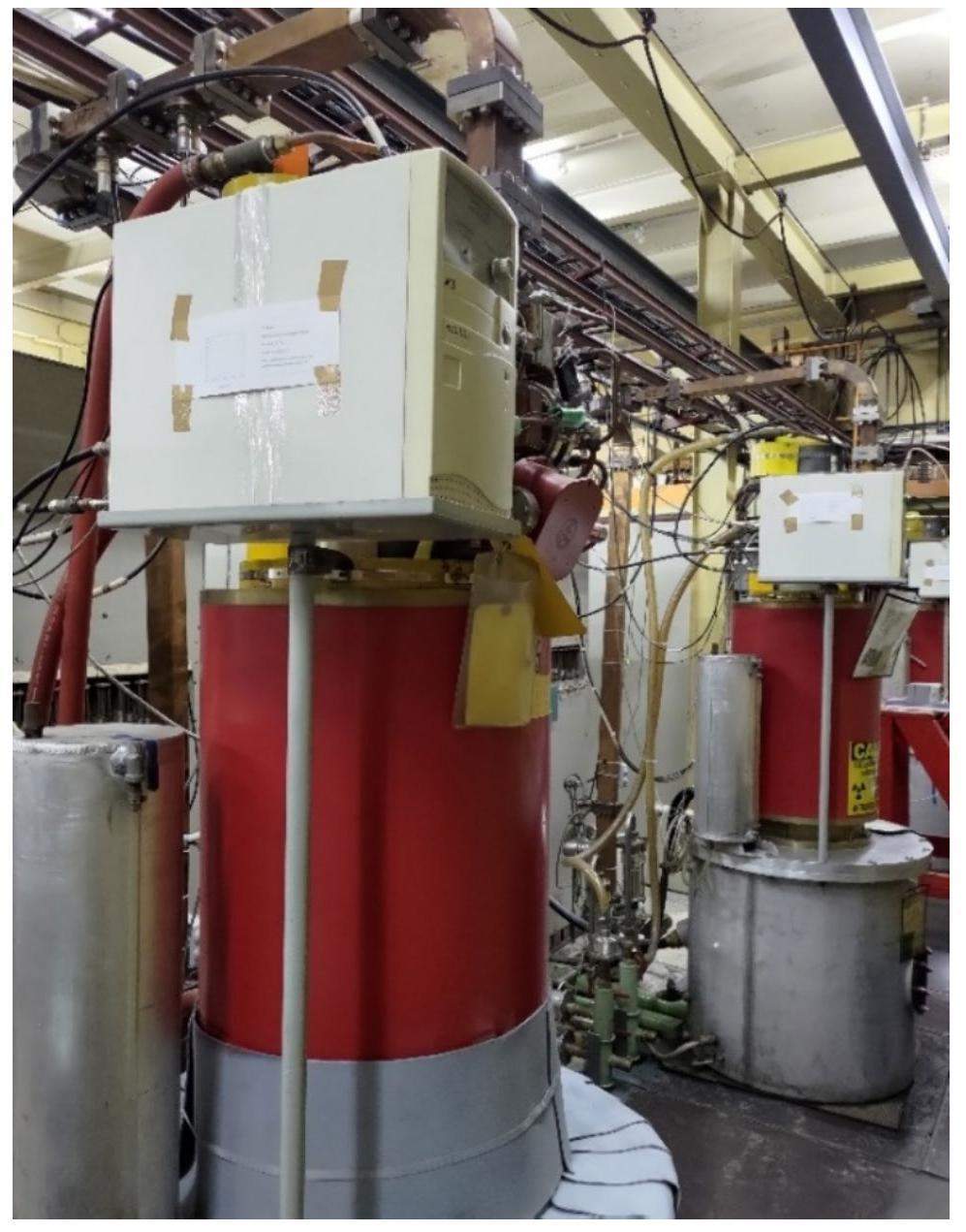
The SLAC 5045 klystron, developed by the Stanford Linear Accelerator Laboratory [2], is depicted in Fig. 1 within the VEPP-5 klystron gallery. Key parameters are outlined in Table 1. Currently, all klystrons are operating in a power-saving mode, delivering a pulse power of no more than 50 MW, with a duration of 3.5 μs and a repetition rate not exceeding 12 Hz. The cathode voltage stands at 350 kV, with a beam current of approximately 350 A. Consequently, it was determined that the klystron under development should closely match these parameters, as listed in Table 2. To minimize the cost of the VEPP-5 upgrade, components such as solenoids, radiation shielding, the thermal stability system, modulator, pulse transformer, etc., are to remain unchanged or undergo minor modifications. It is important to note that while the klystron parameters outlined in Tables 1 and 2 are similar, they are not identical. The klystron under development exhibits lower output power and microperveance.
| Parameter | Value |
|---|---|
| Work frequency (MHz) | 2856 |
| Output pulse power (MW) | 60 |
| Input power (W) | 500 |
| Microwave pulse duration (µs) | 3.5 |
| Repetition rate (Hz) | Up to 120 |
| Beam current (A) | 400 |
| Anode voltage (kV) | 350 |
| Parameter | Value |
|---|---|
| Work frequency (MHz) | 2856 |
| Output pulse power (MW) | 50 |
| Input power (W) | 500 |
| Microwave pulse duration (µs) | 1-3.5 |
| Repetition rate (Hz) | Up to 12 |
| Beam current (A) | 350 |
| Anode voltage (kV) | 350 |
General view of BINP SB RAS klystron
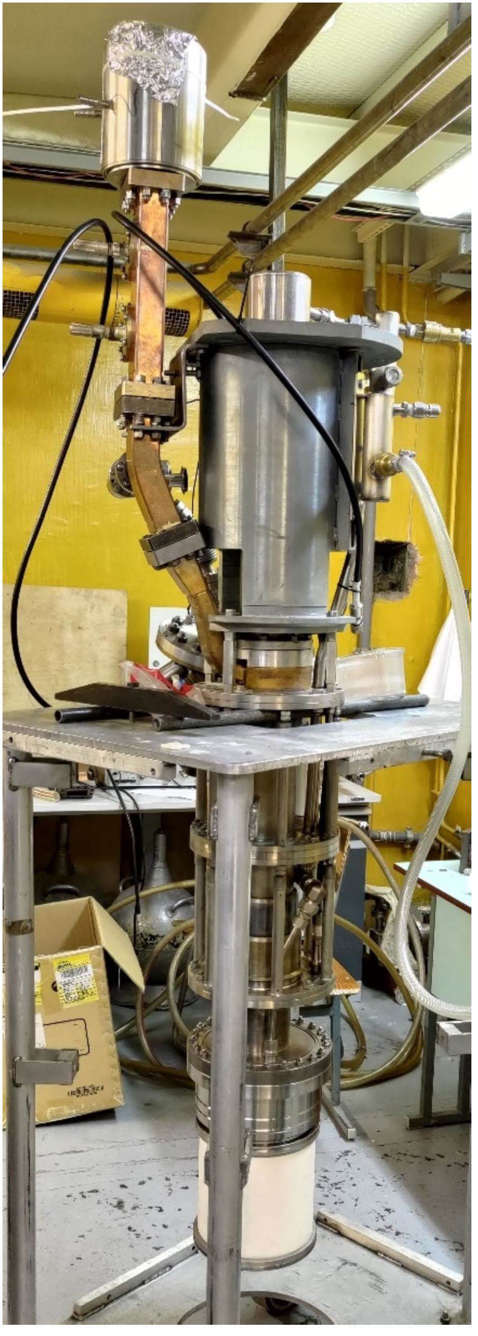
The klystron under development comprises six resonators, including the exciting and output resonators. To facilitate quick replacement of key components, it was decided to construct the klystron prototype as a composite. Therefore, the cathode assembly, bunching system, collector, and output vacuum waveguide window can be replaced independently. All these elements are mounted using vacuum flanges with copper seals. A port is included for continuous vacuum pumping, situated before the output waveguide vacuum window. The appearance of the manufactured klystron is depicted in Fig. 2. This approach eliminates the need for high-temperature bakeout while reducing both the time and cost associated with replacing individual elements.
Cathode unit
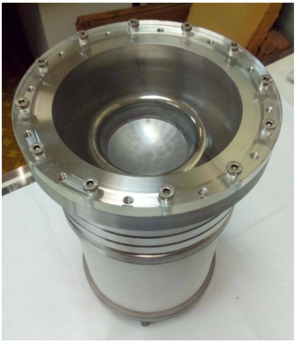
The cathode unit must deliver a current of up to 350 A at an anode voltage of 350 kV. VK-100 (Al2O3 99.7%) ceramics, cylindrical in shape with a height of approximately 200 mm, serves as the high-voltage insulator. The appearance of the cathode unit is depicted in Fig. 3. One side of the cathode unit features a CF-200 vacuum flange, while the other side houses elements of the cathode filament input and adjustment membranes.
The cathode is installed on the cathode "leg" within the cathode assembly, with its position adjustable via adjusting membranes. Filament supply is facilitated through vacuum bushings with ceramic decoupling. The cathode itself, of the dispenser type, features a spherical surface with a diameter of approximately 88 mm. Final treatment of the cathode surface involves turning, removing a layer no thicker than 200 microns. Subsequent to the turning process, optical diagnostics were employed to measure the surface roughness, which registers at a level of 2 to 4 μm. This cathode was manufactured by the Russian company OOO Basic Technologies and Components of Vacuum Devices.
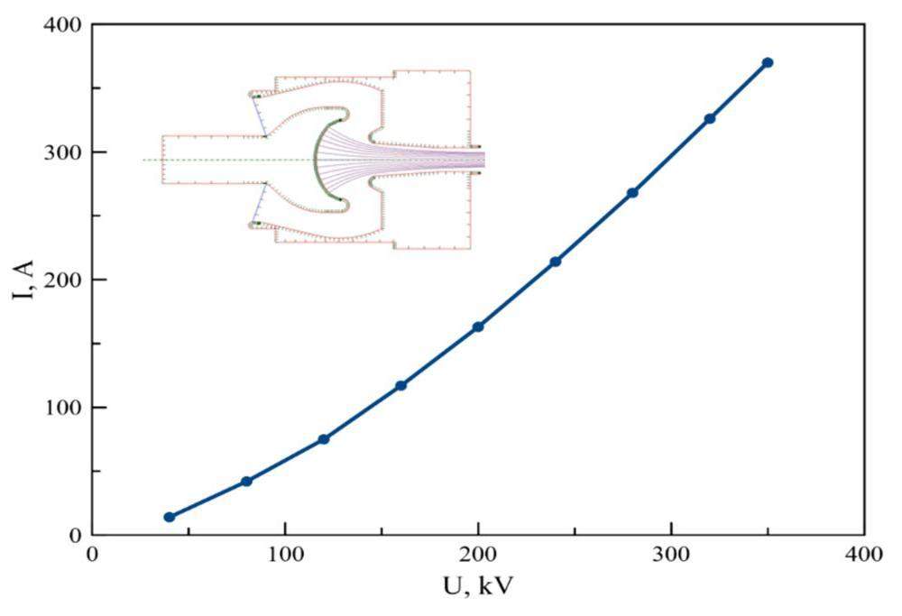
The cathode unit was simulated using two codes: POISSON-2 [8] and ULTRASAM [9], both yielding nearly identical results. The calculated current-voltage characteristic is depicted in Fig. 4, indicating a current of 370 A at an anode voltage of 350 kV. The microperveance was determined to be 1.8 µ A/V3/2.
Before installation into the klystron, the cathode assembly, including the cathode "leg", underwent baking and activation. This process involved utilizing a grid positioned approximately 5–7 mm away from the cathode and heating to a temperature of 1200 °C for activation.
Bunching system
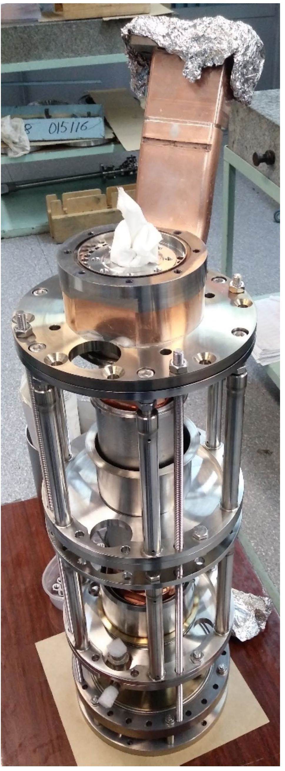
The bunching system comprises the exciting cavity, four passive cavities, and the output cavity. Figure 5 displays the manufactured system for beam bunching. The first cavity contains the exciting loop, connected to the coaxial via the vacuum decoupler. The output cavity links to the waveguide through the coupling window. The cavity is intentionally asymmetrical to counterbalance the distortion of the electromagnetic field induced by its coupling element.
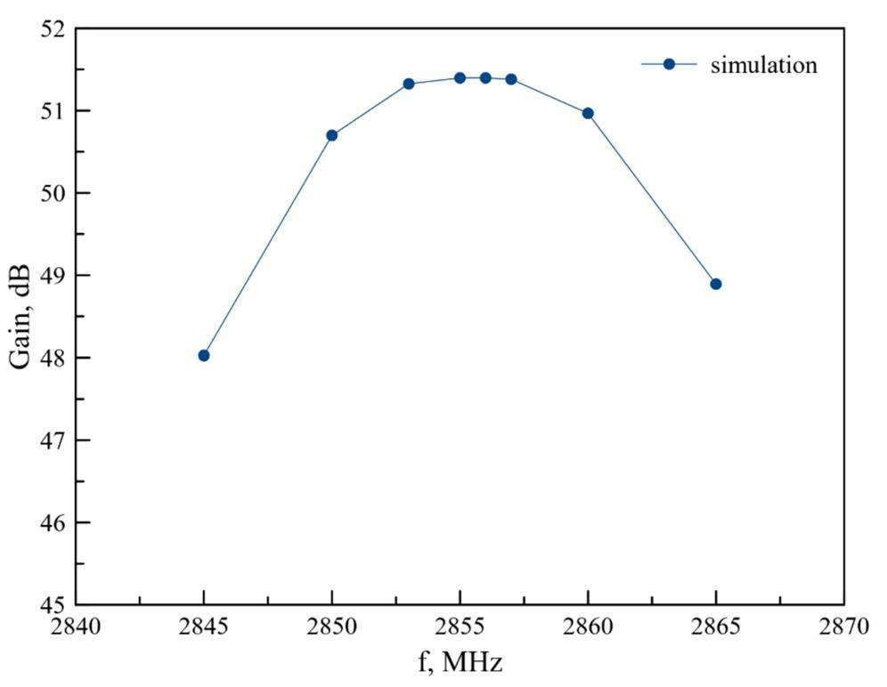
Preliminary calculations for the klystron were conducted using various methods, including analytical approximation [10, 11], one-dimensional code [12], and three-dimensional particle-in-cell code. All calculations indicated a klystron gain of at least 50 dB at the operating frequency, although the band characteristic varied depending on the calculation method. Figure 6 illustrates the klystron band calculated using the particle-in-cell method (CST Microwave Studio [13]).
Klystron collector
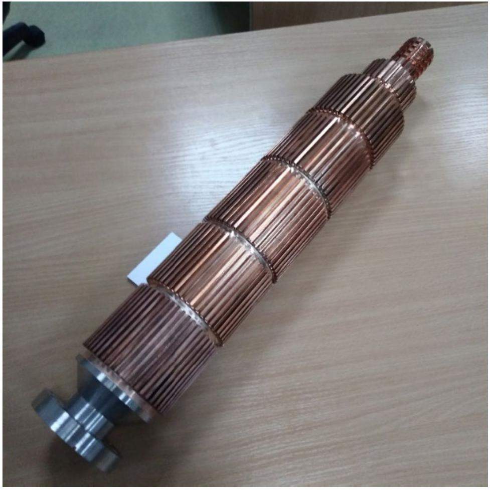
The klystron collector absorbs the transmitted beam and minimizes the backward movement of reflected electrons. Its appearance is depicted in Fig. 7. The outer part is designed with radiator ribs to efficiently dissipate the heat generated by the external cooling circuit that flushes the collector.
Output vacuum waveguide window
The output window of the klystron is a waveguide RF window with a traveling wave in ceramics, also known as a traveling wave window [14, 15]. This waveguide window comprises two input- and output-matched pass-through resonators with the same resonant frequency. These resonators are connected by a section of cylindrical waveguide filled with a dielectric. To input and output microwave power, rectangular waveguides are used, connected through coupling diaphragms. The window operates by the interaction of waves reflected from the coupling diaphragms with rectangular waveguides and waves reflected from the ceramic surfaces, forming a standing wave inside the dielectric-filled resonators. The waves passing through the ceramics on both sides are added in antiphase, preventing a standing wave within the ceramics. The ceramic material used is AL2O3 (99.7%). No conductive coating is applied to the ceramic, partly due to the lack of such technology at BINP SB RAS, but also because previous experience has shown that the absence of a coating does not necessarily lead to rapid breakdown of the window. Nonetheless, the window is designed to be quick-removable, allowing for easy replacement in case of failure.
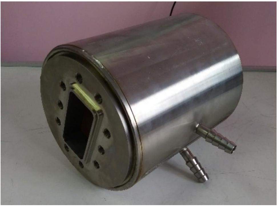
This window type transmits high power levels by minimizing electric fields in the ceramic region, unlike a classic pill-box window. As a result, a single traveling wave window can replace a waveguide splitter-combiner with two pill-box windows. Installed using waveguide vacuum flanges and water-cooled, the window (refer to Fig. 8) maintains a voltage standing wave ratio (VSWR) within the klystron's operating frequency band that does not exceed 1.2.
Magnetic field
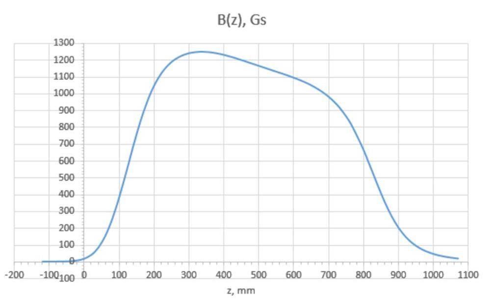
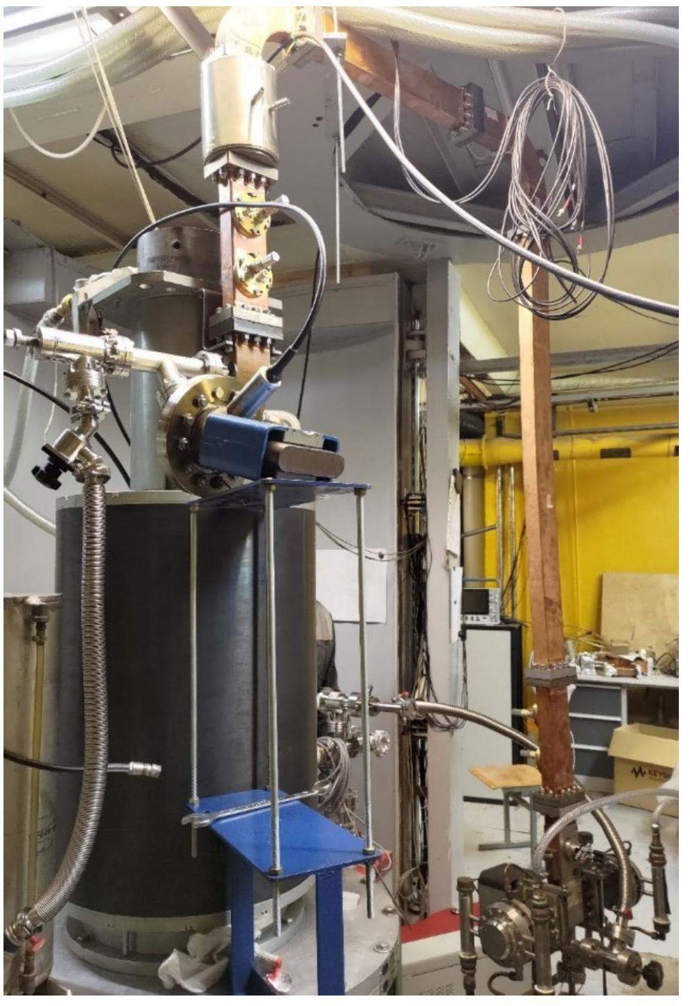
The klystron's magnetic field is produced by a solenoid. Since the accelerator complex already has the necessary engineering infrastructure for 5045 klystron solenoids, a similar solenoid was manufactured. Its distinctive feature is the formation of a non-uniform magnetic field due to several coils that are powered in series from a single current source (Fig. 9). Figure 10 displays the manufactured solenoid, while Fig. 9 illustrates the measured magnetic field distribution along the axis, with the zero-coordinate coinciding with the cathode's position. These measurements correspond to a current source of 15 A.
Results
Figure 10 depicts the setup for testing the klystron. The output power reached the matched water load through a calibrated waveguide coupler positioned beforehand. Just before the waveguide vacuum window, there was an uncalibrated coupler to observe the processes occurring within the window. The klystron was housed in an in-house solenoid, designed similarly to the SLAC 5045 klystron's solenoid. High voltage was delivered via a pulse transformer housed in an oil tank. High voltage pulses were generated using the modulator's pulse forming network, while the cathode filament was supplied by the filament transformer.
Before being installed on the stand, the klystron was heated to a temperature of 120°C, which was insufficient to achieve high vacuum levels. This temperature limitation was due to the presence of vacuum flanges with copper seals, among other technological constraints. The final processing, including the simultaneous activation of the cathode, occurred on the stand. However, due to inadequate preheating, this process took an extended period.
High voltage processing commenced at the beginning of February 2023. By the end of February, the first RF signal pulse was generated. It's worth noting that prior to the stand's commissioning, processing of the output vacuum waveguide window was not possible, significantly impacting the klystron's transition to operational mode. In the latter half of March, the targeted output power of 50 MW was achieved with an RF pulse duration of 0.3 μs. Consequently, the klystron operated almost continuously until July 2023, consistently delivering the nominal power output at frequencies up to 5 Hz and a pulse duration of 1.5 μs. The pulse duration is constrained by the anode voltage duration, and increasing it requires upgrading the modulator's shaping line. The vacuum waveguide RF window facilitated the transmission of the attained power level.
The vacuum level within the klystron was suboptimal, approximately 10-8 Torr along the output waveguide transmission line, with no means to gauge the vacuum level in the cathode region. Consequently, an increase in repetition frequency could lead to high-voltage breakdowns due to vacuum deterioration and inadequate conductivity of the pumping path. In simpler terms, transitioning to higher average power necessitates continued klystron processing. Despite these challenges, the emissive properties of the cathode remained intact. Following a high-voltage breakdown, cathode emission would promptly recover. Upon restoring the vacuum to operating levels, there was no alteration in emission current upon reactivating the high voltage.
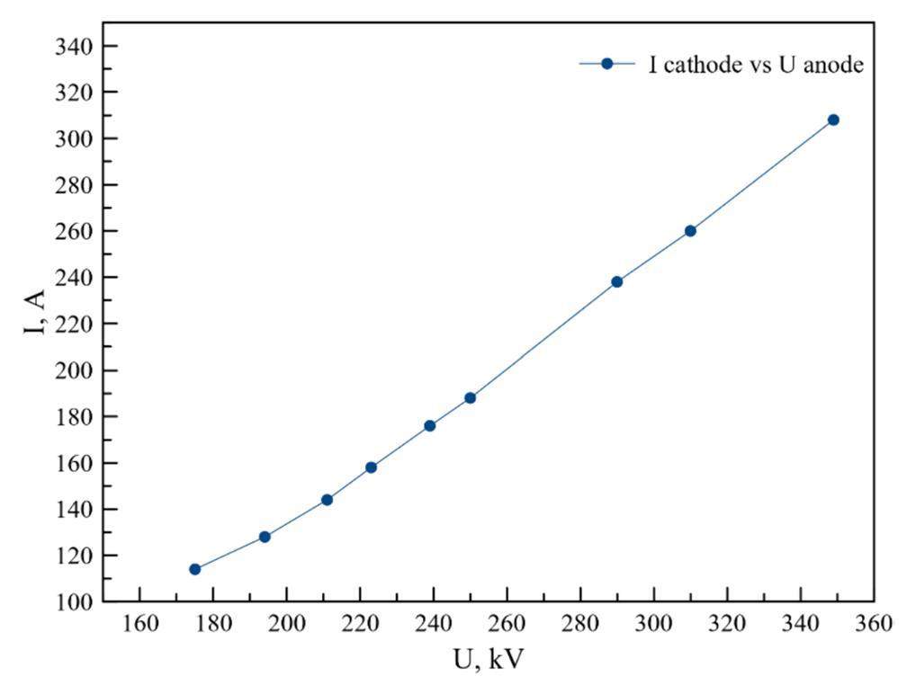
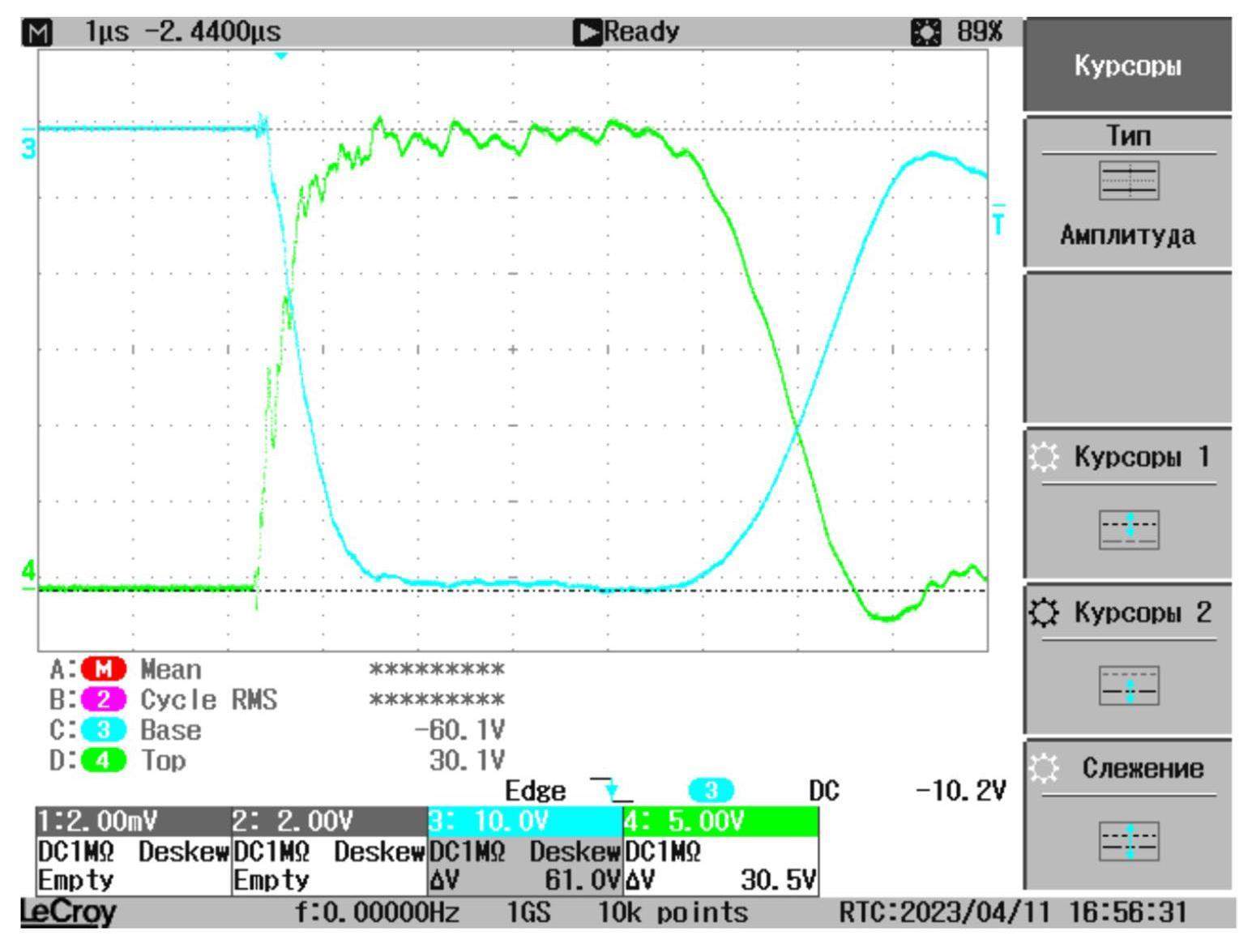
Figure 11 depicts the current-voltage characteristic obtained from the data, indicating that the resulting current is lower than the calculated one (refer to Fig. 4). The measured microperveance was 1.5 µA/V3/2, compared to the calculated 1.8 µA/V3/2. One potential reason for this discrepancy could be the incorrect positioning of the cathode relative to the anode. Further calculations revealed that a 1 mm shift in the cathode-anode distance reduced the microperveance from 1.8 µA/V3/2 to 1.5 µA/V3/2. Apart from the accuracy of aligning the cathode assembly, the cathode-anode distance is influenced by thermal expansion. Thermal calculations conducted in CST Microwave Studio showed a temperature gradient of approximately 240 degrees from the base of the cathode assembly to the end of the near-cathode electrode, resulting in a decrease in the cathode-anode distance of about 0.6 mm when heated. As previously mentioned, the cathode unit is affixed to the vacuum flange. Despite the presence of adjustment membranes for aligning the cathode "leg," it is impossible to measure the cathode-anode gap after the unit is installed. Thus, any initial assembly error within the vacuum insulator could lead to a reduction in cathode emission output. However, the attained current of 310 A is adequate for klystron testing. Figure 12 illustrates a high-voltage pulse and the beam's current pulse.
The output power was measured using a calibrated waveguide coupler before the matched load, along with a calibrated detector. To achieve maximum output RF power, which is significantly influenced by the accompanying magnetic field, the optimal solenoid current was selected. A decrease in the magnetic field by approximately 15% resulted in an increase in output power. However, beyond a certain level, self-excitation processes of the beam could occur. These processes involve excitation in the first resonator and excitation of higher modes in the grouping channel. The first process likely arises from secondary emission discharges occurring in the first resonator when the beam's field is weakened too much. Higher modes in the bunching channel may also be attributed to reduced beam density or inaccuracies in cathode alignment. It's noteworthy that no self-excitation effects are observed at the klystron's operating parameters. Figure 13 illustrates the measured dependence of output RF power on input power.
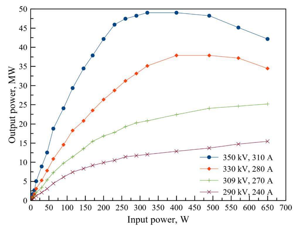
Figure 13 indicates that the RF output power reached approximately 50 MW. Considering the calibration accuracy of the waveguide coupler, we can estimate a measurement accuracy of about ±8%. This precision results from the output waveguide coupler, which features a relatively low tap ratio of less than -70 dB. Prior to installation in the output waveguide path, this coupler underwent calibration. Following cessation of klystron operation, the waveguide path was disassembled, and the coupler was rechecked for tap ratio accuracy, yielding a result of 0.6 dB. The graphs in Fig. 13 illustrate saturation occurring at an input power exceeding 400 W. The pulse duration was 1.5 μs, limited by the duration of the anode voltage. Figure 14 depicts the envelope of the microwave pulse from the RF detector.
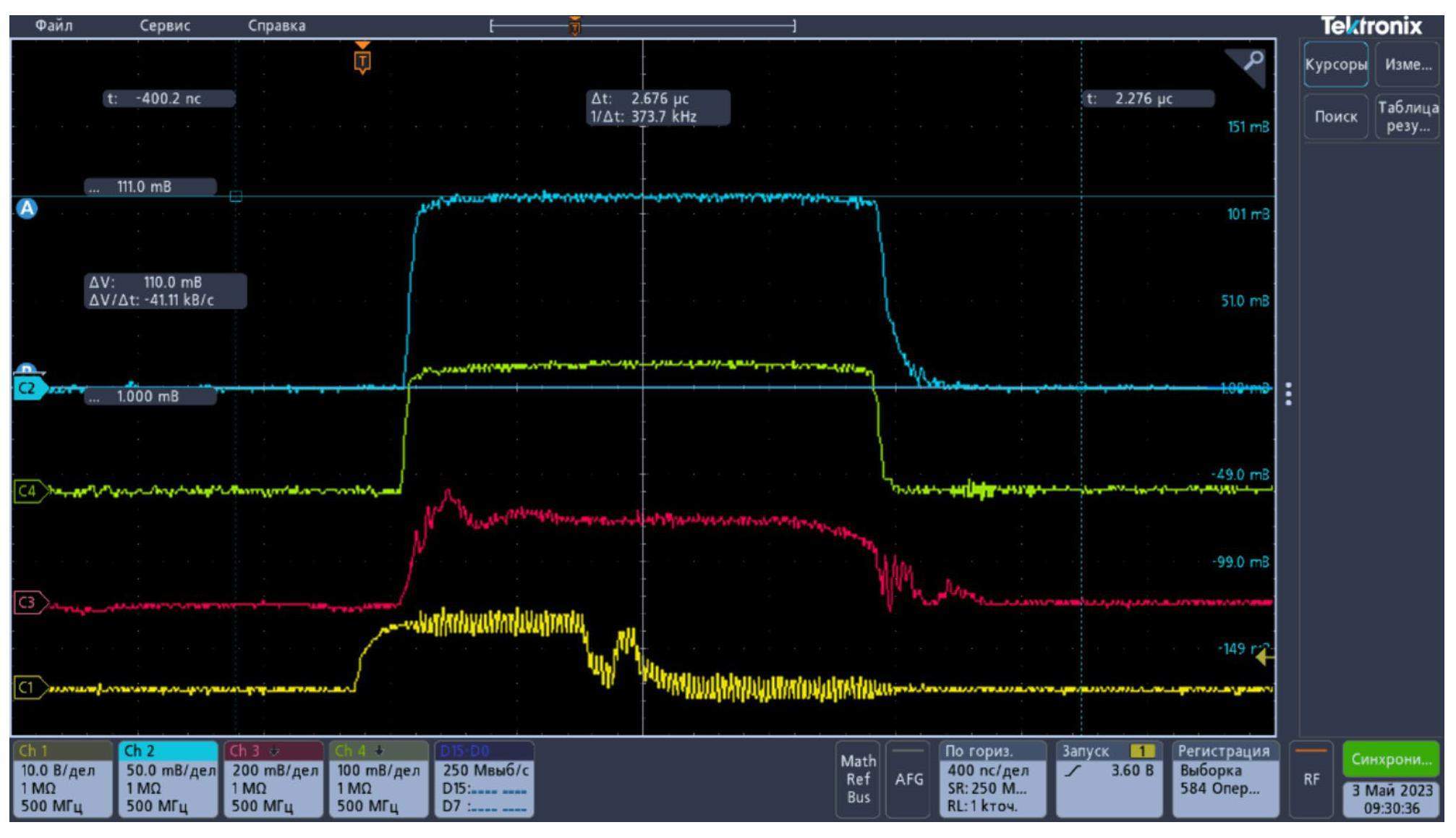
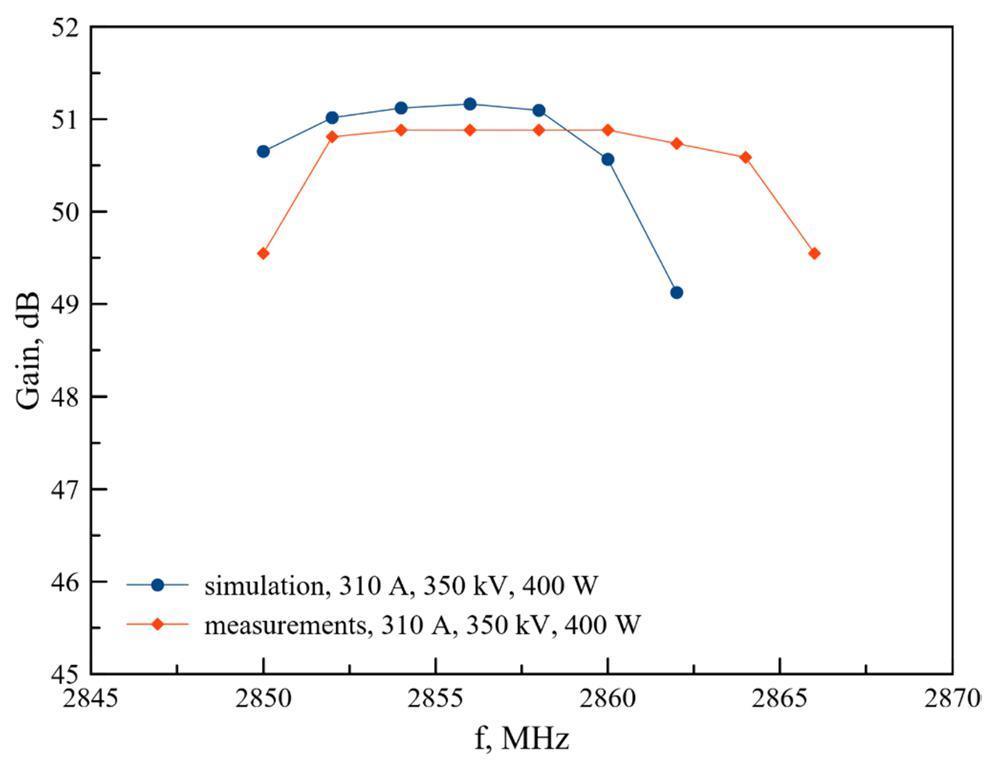
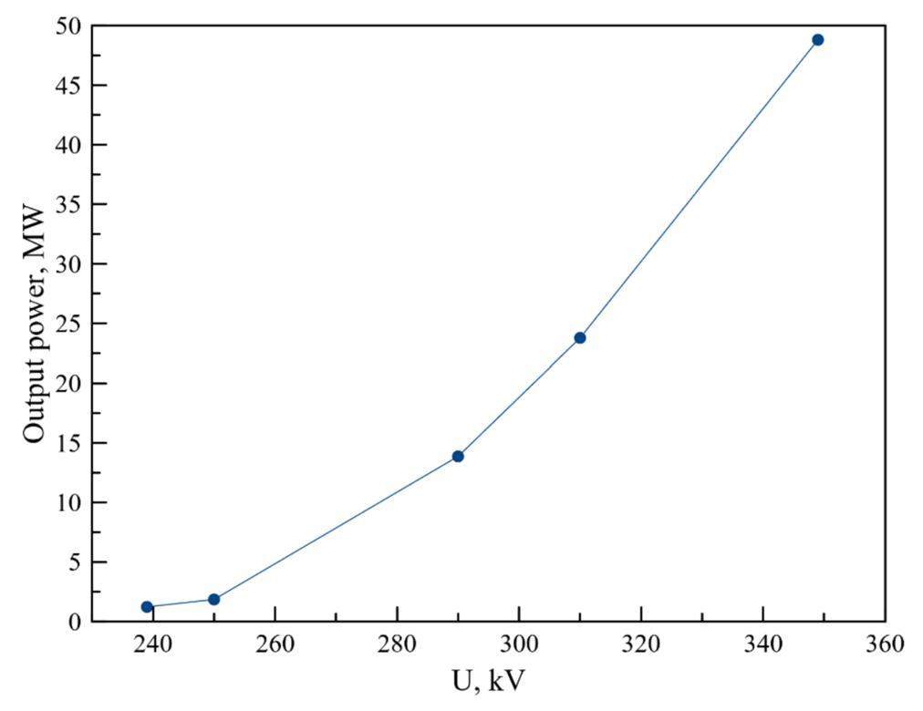
Figure 15 illustrates the klystron band, while Table 3 presents the overall parameters achieved. Calculations depicted in Fig. 6 and measurements were conducted at different beam currents: calculations at 350 A (microperveance 1.8 µA/V3/2), and measurements at 310 A (microperveance 1.5 µA/V3/2). In Fig. 15, a new simulation is presented with a beam current of 310 A. During bandwidth measurement, a "shelf" of output power was observed within a certain frequency range. One possible explanation for this phenomenon is insufficient measurement accuracy, which, as mentioned earlier, is within several megawatts, impacting the data obtained. Additionally, it's apparent that the center of the measured band slightly shifts toward higher frequencies. While this does not hinder operation at 2856 MHz, it may suggest that the frequency characteristics of the grouping resonators are suboptimal for a beam current of 310 A. Further investigation into these issues will continue, and adjustments may be made for future instances of the klystron. Figure 16 illustrates the dependence of output power on anode voltage.
| Parameter | Value |
|---|---|
| Work frequency (MHz) | 2856 ± 4 |
| Output pulse power (MW) | 50 ± 4 |
| Input power (W) | 350 |
| Microwave pulse duration (µs) | 1.5 |
| Gain (dB) | 51.5 |
| Efficiency | 46% |
| Repetition rate (Hz) | up to 5 |
| Beam current (A) | 310 |
| Anode voltage (kV) | 350 |
Conclusion
The first fully manufactured prototype of a klystron, capable of delivering approximately 50 MW of RF output power at an operating frequency of 2856 MHz, was completed at BINP SB RAS. This involved completing all design stages: calculations, design, technology development, manufacturing, tuning, and testing. While some features of the prototype hinder achieving high vacuum, they significantly simplify and reduce the cost of the manufacturing process. Consequently, there are limitations on testing with high average power. However, the achieved parameters already allow operation with linear accelerators where high performance is unnecessary, such as injectors of synchrotron radiation sources. The results obtained indicate that the klystron parameters and technological solutions were chosen correctly, paving the way for serial production. Some issues, including improving measurement accuracy, klystron bandwidth, and achieving higher perveance, will be studied and possibly adjusted. Nevertheless, the performance of the manufactured klystron prototype has been demonstrated. Building upon the prototype, a fully functional implementation of the klystron will be developed, suitable for both existing and future complexes with linear accelerators. This klystron will feature exclusively soldered and welded seams to ensure high vacuum and expedite processing. Additionally, the developed klystron prototype will serve as an RF test stand for processing and testing various elements of linear accelerators at high levels of RF power output.
VEPP-5 Injection Complex
. Phys. Part. Nuclei Lett. 20, 754-756 (2023). https://doi.org/10.1134/S154747712304025825 Year performance review of the SLAC 5045 S-band klystron
. in Proceedings of the 11th International Particle Accelerator Conference IPAC2011,SLED: A Method of Doubling SLAC’s Energy
, in Proceeding of the 9-th International Conference on High Energy Accelerators,Development of 200 MeV linac for the SKIF light source injector
. J. Inst. 17, T02009 (2022). https://doi.org/10.1088/1748-0221/17/02/t02009Conceptual design of a dedicated fourth-generation specialized synchrotron radiation source (SSRS-4) at the kurchatov institute
. Phys. At. Nucl. 81, 1646-1651 (2018). https://doi.org/10.1134/S1063778818110030Numerical solving of integral equations of the potential theory in the electron optic problems
. PhD thesis,ULTRASAM-2D code for simulation of electron guns with ultra high precision
, in Proceeding of Europe Particle Conference EPAC2002,Method for solving multidimensional problems of optimizing the parameters of high-power klystrons
. In Proceedings of 19th International Asian School-Seminar on Optimization Problems of Complex Systems (OPCS),High-power tests of pill-box and TW-in-ceramic type S-band RF window
, in Proceedings of the 1994 International Linac Conference, Tsukuba, Japan (1994), pp. 457-459Waveguide window
. Pat. No.The authors declare that they have no competing interests.

