Introduction
Cosmic-ray (CR) detection is at the forefront of intense research and is represented by sophisticated experiments dedicated to clarifying their origin, acceleration, and propagation mechanisms in the universe [1, 2]. Considerable insights have been obtained from the investigation of CRs over the past decades, leading to a deeper understanding of the intrinsic interactions constituting the fields of particle and astroparticle physics. Although important results have been obtained by indirect (ground-based) experiments, highly energetic CR particles from GeV to PeV energies and gamma rays need to be explored via direct observations using space-borne instruments.
The High-Energy Cosmic-Radiation Detector (HERD) is a space-borne instrument that will be installed onboard the Chinese Space Station (CSS) in 2027 [3, 4]. The main scientific objectives of HERD include the search for signals of dark-matter annihilation products, the precise measurement of the CR spectrum and composition up to knee energy, and high-energy gamma-ray monitoring and surveying [5-7]. The data gathered from the HERD detectors can provide valuable information for developing radiation-shielding technologies and mitigating the risks posed by cosmic radiation during long-duration space missions. The HERD project has significant implications for fundamental physics research. Researchers can probe the boundaries of particle physics by studying the properties of CRs.
HERD is designed around a segmented, three-dimensional imaging calorimeter [8-11]. This design ensures the detection of impinging radiation from the top and the four lateral sides. Above the calorimeter, a silicon tracker is placed on the top active sides [12]. Subsequently, a plastic scintillator detector covering the calorimeter and tracker provides gamma-ray and charged-particle triggers, together with an additional level of charge measurement [13, 14]. Additionally, a silicon charge detector (SCD) comprehensively covers all subdetectors to further enhance the charge-measurement precision [15]. A transition radiation detector is placed on one of the lateral faces of HERD to calibrate the energy of the nuclei in the TeV region. Consequently, an order-of-magnitude upgrade in acceptance can be obtained by a novel design with advanced detector techniques that fulfill all physics requirements while maintaining a manageable payload for a space mission. For the first time, an acceptance > 3 m2 sr for electrons and gamma rays and > 2 m2 sr for protons and nuclei will be achieved in a space mission, which will ensure the collection of significative statistics up to the highest energies.
Silicon-strip detectors are widely used in high-energy physics, nuclear physics, and space missions because they have low noise, good linearity, and excellent position and energy resolution [16-20]. Therefore, the SCD is based on several silicon-strip detectors. The SCD is the outermost detector of the HERD and is required to detect the CR charge from Z = 1~28 with resolution typically better than 0.3 c.u. @ Z = 6. In physics, Z refers to the atomic number, and c.u. is used as a unit of charge measurement, referring to the charge of one electron. The flight configuration of the SCD consists of five thin detector units. One unit, the SCD placed on the top, has an active area of a 1.536 m×1.536 m square, whereas the other units, the SCDs situated on the sides, are measured at 1.536 m×0.768 m. Each SCD unit comprises eight layers of single-sided silicon-strip detectors. The numbers of silicon-strip detectors used for each layer are 256 and 128 at the top and sides, respectively. The total active area of the SCD is approximately 60 m2. Adjacent layers are installed in orthogonal directions to identify the charges and trajectories of incoming charged particles. This selection ensures that a low level of CR nucleonic fragmentation can be achieved, leading to a decrease in systematic uncertainties while providing vital charge measurements [21, 22]. Each orthogonal-plane pair is composed of a supporting structure consisting of carbon-fiber skins and an aluminum honeycomb core.
An ASIC is chosen as the front-end readout chip to read a large number of detector signals (approximately 500000 channels). The highlight of this study is the expansion of the dynamic range from 200 fC to 1200 fC. We also study charge sharing in silicon-strip detectors to facilitate the detection of particles with Z = 28 [23]. To evaluate the performances of the SCD detectors in the beam test, we develop a set of readout electronics for the SCD prototype. In this study, we first briefly introduce the SCD prototype and present the detailed design of the readout system. The test results are then presented. By analyzing and presenting the test results in detail, we evaluate the performance of the readout system of the SCD prototype.
SCD prototype
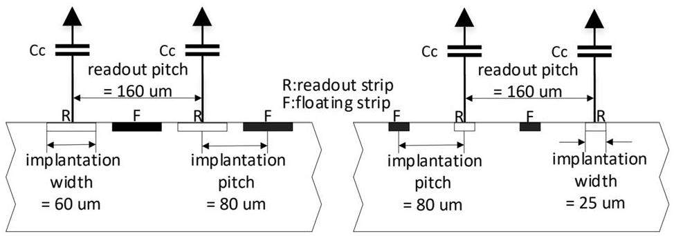
The detector prototype is composed of an AC-coupled single-sided silicon-strip detector with an active area of 6 cm×3.2 cm and a thickness of 320 μm. The thickness of the silicon is chosen as a compromise between the detection efficiency of incident particles, which requires high thickness, and the noise induced by the collection of charges produced by the interaction of the charges, which increases with increasing thickness. Figure 1 illustrates the cross section of a silicon sensor. The surface of the silicon-strip detector is a layer of P+ silicon microstrips covered with a thin aluminum film, with N-type silicon serving as the sensitive area of the detector, and a heavily doped N+ layer and backside electrode at the bottom [24]. By applying a sufficiently large reverse voltage to the bar-shaped PN junction, the concentration of the drift-charge carriers inside becomes very low. At this point, the electric field in the sensitive area follows an approximately linear distribution, and the amount of charge absorbed by the electrode is proportional to the energy deposited by the incident particles [25]. The SCD has 400 implant strips with a pitch of 80 µm. Two regions with different implant-strip widths exist: one is 60 μm and the other is 25 μm. The internal-coupling capacitances are 575 pF and 241 pF. The full depletion voltage of the SCD is approximately 30 V and the operating bias voltage is set to 80 V. To reduce the number of readout channels while maintaining satisfactory performance in terms of spatial and charge resolution, readout is performed using the floating-strip approach, where a particular number of implanted strips are not read out [26, 27]. When high-energy particles hit the silicon-strip detector and interact with the sensitive area, the deposited energy generates electron-hole pairs. Under the influence of an external electric field, the electrons and holes drift in two directions, and the silicon strips rapidly collect charge information, which is used to infer the trajectory and energy of the incident particle [28, 29]. In the HERD project, multiple silicon-strip detectors are cascaded into arrays to increase the detection area [30, 31].
To achieve low power consumption and high integration, the prototype electronics are divided into two parts: front-end readout electronics (FEE) and back-end data acquisition (DAQ), as shown in Fig. 2.
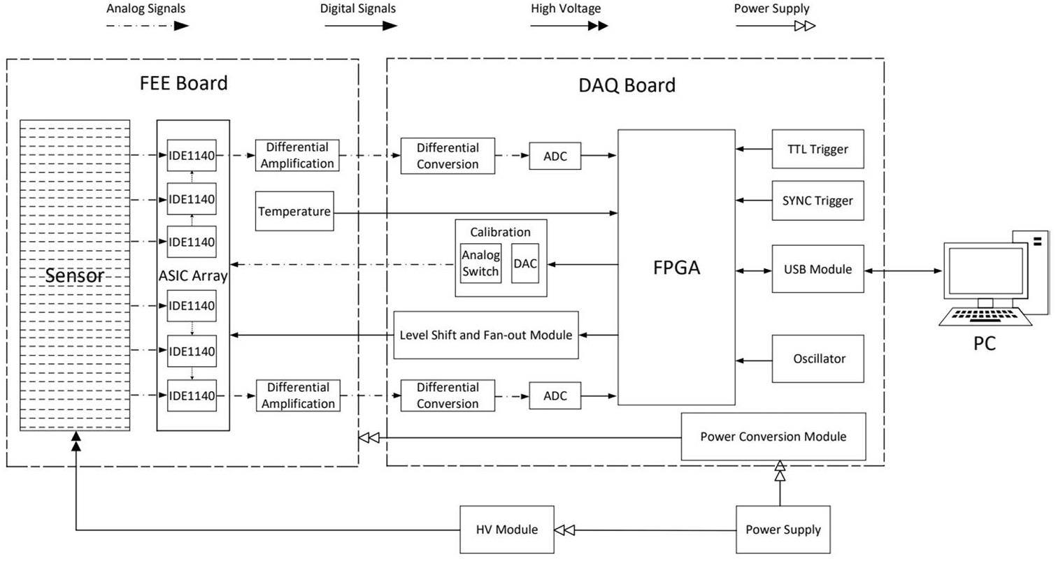
The FEE board comprises a silicon-strip detector, two sets of ASIC arrays, two sets of differential-amplification circuits, and a temperature-acquisition module. Three ASICs are cascaded into an array to amplify and read charge signals from the SCD. The differential-amplification circuits process the differential analog current signals output by the ASIC array before they enter the DAQ board. Temperature changes affect the detector performance. Generally, as the temperature increases, the resistivity of silicon decreases and the rate of carrier generation increases, which may lead to increased noise or decreased detector sensitivity. Thus, the temperature must be measured and the relationship between the temperature and performance must be analyzed.
The DAQ board consists of two sets of differential conversion modules, two sets of analog-to-digital convertor (ADC) modules, calibration modules, ASIC control-signal-level conversion and fan-out modules, an field-programmable gated array (FPGA), TTL trigger modules, synchronous trigger modules, USB modules, power-conversion modules, and high-voltage modules. Acting as the central processing unit, the FPGA governs the entire electronic system by receiving and relaying commands from the host computer, packaging the scientific data, and transmitting them to the host computer.
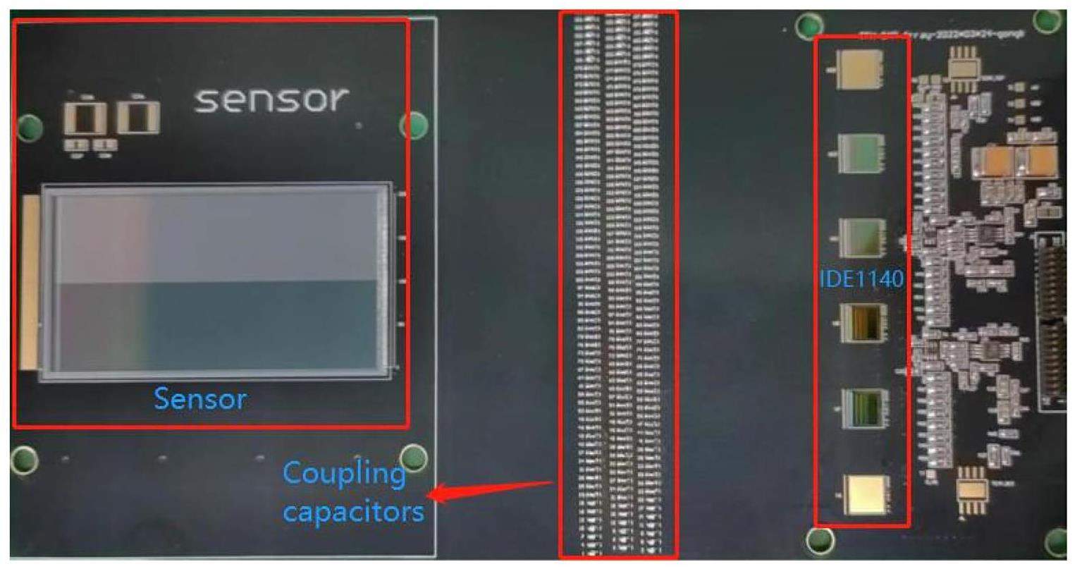
The SCD and charge-sensitive preamplifier IDE1140, produced by IDEAS, are bonded to the FEE circuit board using a conductive adhesive [32]. Using a fully automated wire-bonding machine, the pins of the SCD and IDE1140 are wire-bonded to the solder pads on the PCB to establish electrical connections. The dimensions of the unpackaged die IDE1140 are 6.5 mm×6.2 mm, with 64 wires laid out within the 6.2 mm width of the chip. The spacing between adjacent wires is less than 100 μm, balancing the processing difficulty of the PCB and robustness of the bonding. The solder pads utilize a chemical nickel-palladium-gold process to prevent oxidation and enhance the stability of wire bonding.
The silicon-detector section requires shading protection, and the entire FEE board must be sealed inside the shielding enclosure. A shielding enclosure was designed for the FEE with a carbon-fiber exterior. This design provides both protection and light shielding. Moreover, carbon fiber has a low mass-to-weight ratio, ensuring minimal impact on the incident radiation. During the beam experiments, the beam strikes a fixed area on the silicon detector. To reduce the mass, the back side of the silicon detector on the FEE is hollowed out.
The following sections provide a detailed introduction to the design of the FEE and DAQ. In addition, a minimum front-end readout board (miniFEE) was designed to test the dynamic range and load noise. Only one ASIC is wire-bonded to the miniFEE board without silicon detectors.
Front-end design
The main function of the FEE is to amplify the analog signal detected by the silicon-strip detector. The FEE is composed of two ASIC arrays and differential-amplification circuits, as shown on the left-hand side of Fig. 2.
IDE1140 is selected as the front-end readout chip considering its dynamic range, noise level, and power consumption. This chip has 64 readout channels, a large dynamic range (-200 fc to +200 fc), low noise (139 e- for a 0 pF input), and low power consumption (0.29 mW/channel). This chip implements 64 parallel charge-sensitive preamplifiers (CSAs) and a shaper circuit with a multiplexed analog readout, calibration facilities, and internally generated biases [33]. The pulse heights from all the channels can be sampled simultaneously and switched to one differential analog current-output buffer via an analog multiplexer. In the FEE, three IDE1140 chips are connected in a daisy chain.
Figure 3a shows the architecture of IDE1140 [34]. The normal and test modes of IDE1140 can be controlled externally by a “test_on” signal. In the normal mode, the 64 inputs are connected to a sensor that delivers electrical charges to the pre-amplifier inputs. In the test mode, the sensors do not need to be connected. This mode connects the pulse input generated by the DAC circuit to the cal pad via a switch controlled by a bit register. In addition, in this case, only one channel can be calibrated simultaneously. The chip includes a 2 pF calibration capacitor for testing. When an electron-hole pair is formed in the silicon detector, charge signals are injected into the corresponding IDE1140 input channel. These signals are amplified by the CSA and then passed through a slow shaper circuit to broaden the signal peak, forming a Gaussian-like signal. The “hold” signal is used to control the sample-and-hold circuit, which holds and samples the Gaussian-like signal at its peak by setting an appropriate hold time. Typically, after the peak is reached (6.5 μs), an external “hold” signal should be applied to sample the value. The outputs of the 64 channels can be switched in the multiplexer that is controlled by the bit register. The “shift_in_b” and “ckb” signals are used to control the bit-register, which can perform a sequential read-out. The multiplexer output is buffered and can be read out at the “outp” and “outm” signals. Only one of the switches in the mux can be “on” at a time; thus, the chip output can only display one channel at a time. The logic part of the chip can be reset either by applying “dreset” or simply by running through a normal read-out once.
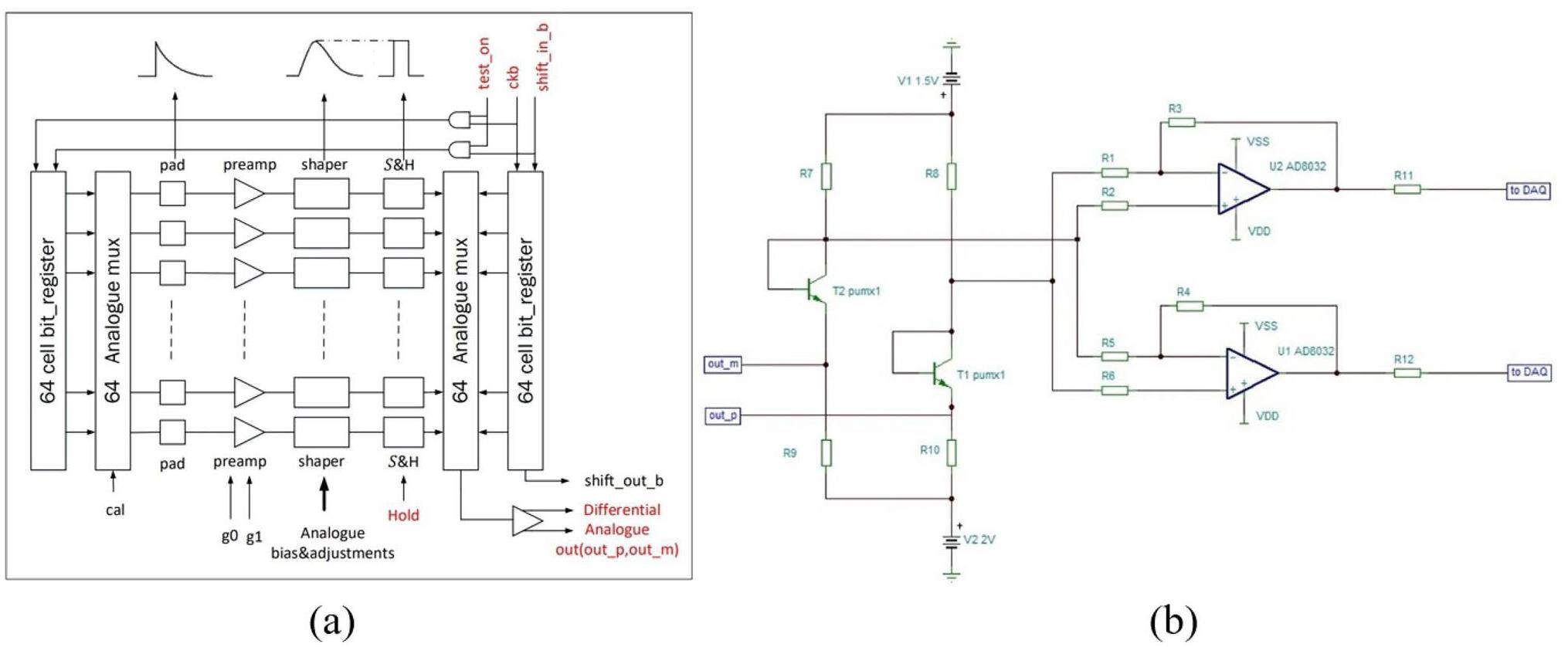
The differential current signals from the ASIC are amplified and converted into a pair of differential voltage signals using the differential-amplification circuit, as shown in Fig. 3b. The differential current signals output by the ASIC are individually directed to a transistor, which convert the current signals into voltage signals. Subsequently, they enter differential-amplification circuits, where the signals are amplified to fit within the voltage range of the ADC, thereby maximizing the utilization of the dynamic range of the ADC. Decreasing the resistance values of feedback resistors R3 and R4 can diminish the gain of the front-end circuit, thereby expanding the dynamic range of the measurement. During signal transmission, the signal lines may encounter electromagnetic interference or other external disturbances, resulting in additional noise on the signal lines. The utilization of differential-amplification circuits aids in reducing common noise caused by factors such as poor grounding and power supply.
Back-end data-acquisition and control system
DAQ design
The DAQ input requires a connection to a silicon charge detector with a scientific data-output rate of 10 Mbps, and the external trigger enters the DAQ through the I2C interface. Analog–to–digital conversion, data packaging, the charge-injection function, and data transmission are all performed using the DAQ. The DAQ board includes an FPGA, ADC module, calibration module, trigger module, USB communication module, and power-supply module. The Xilinx FPGA chip XC3S500E is selected as the main control chip. The ADC chip is an AD7476 with a 12-bit serial output, which has a throughput rate of 1 MSPS and a power consumption of only 3.6 mW [35]. This ADC chip ensures high precision and efficiency in converting analog signals into digital data. For USB communication, the DAQ system relies on the Cypress CY7C68013A chip. This selection is based on its suitability for USB-interfacing tasks, providing reliable and high-speed communication between the DAQ board and host computer. This chip ensures the timely and accurate transfer of experimental data for further analysis and processing.
The DAQ-operation logic consists of four modes: self-triggering, calibration, synchronous external triggering, and TTL external triggering. The self-triggering mode uses a 50 Hz periodic signal generated by the FPGA as an internal trigger source. This mode tests the system for proper operation and acquires the pedestal data through multiple events. The calibration mode uses a 10 kHz trigger signal generated by the FPGA to calibrate the range of the measured charge in the system and determine the linearity of the system. The FPGA controls the IDE1140 to select the test mode. The host system permits the adjustment of calibration pulses with amplitudes ranging from 0 V to 2 V. These commands are decoded and forwarded to the FPGA via USB. Subsequently, the FPGA is responsible for configuring the parameters of the calibration circuit. Two trig modes are used for both the standalone and beam tests. For the standalone test, a simple TTL signal is sufficient. The external +3.3 V trigger signal can be directly input to the FPGA through an SMA connector. For the beam test, the trig signal from the trigger system with the I2C protocol is used, which includes the trigger number and trigger type to ensure accurate synchronization and control.
The analog-to-digital conversion circuit is responsible for digitizing the differential signals output by the front-end electronics and transmitting the data to the FPGA unit. Initially, the differential signals from the front-end electronics are converted into single-ended signals using an operational amplifier. Subsequently, the converted signals are digitized using a 12-bit serial ADC chip, AD7476, as shown in Fig. 4a. Biasing is applied to the operational amplifier during the conversion of differential signals into single-ended signals, ensuring that the converted signals fall within a suitable ADC dynamic range. The sliding resistor adjusts the pedestal. The DAQ board has two sets of differential conversion circuits and ADCs, each set corresponding to three IDE1140 chips. The utilization of the serial ADC chip AD7476 stems primarily from power-consumption considerations. Given that the total number of readout channels in the SCD is approximately 500000, necessitating 1500 ADC chips, the power consumption of each ADC chip significantly affects the overall system power consumption. Hence, AD7476, with a power consumption of only 3.6 mW (at a sampling rate of 1 MSPS with a +3 V power supply), was selected owing to its low power-consumption characteristics.
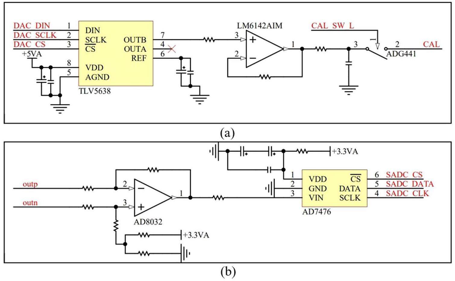
As depicted in Fig. 4b, a calibration circuit is utilized to inject pulses of varying amplitudes into the IDE1140 during the test mode [36]. During system testing, a stable level is initially output by the serial DAC chip TLV5638 to adjust the amplitude of the pulse signal [37]. The output voltage of TLV5638 remains linear within the range of 0-2 V, effectively covering the dynamic range of IDE1140. Subsequently, pulse signals are generated by opening and closing the analog switch ADG441. The step pulse signal is input to the calibration pin of the IDE1140. A first-stage buffer is interposed between the serial DAC and analog switch to enhance the signal-driving capability. Using a 2 pF coupling capacitor integrated with IDE1140, the calibration circuit simulates external charge injection. Only one channel can be calibrated simultaneously. All the channels can be tested by changing the analog switch and “ckb” signal sequentially.
The scientific-data packet includes a packet header, 384 channels of ADC values, temperature values, the version number, the trigger ID, trigger types, trigger-sequence numbers, and the packet end. The data packet is 512 × 16 bits in length and is stored in the FIFO of the FPGA.
The FPGA logic design corresponds to hardware functionalities, primarily comprising the main control logic, reset and clock management, IDE1140 control, ADC control, calibration-pulse generation, trigger management, and USB communication. The main control logic decodes the commands received from the USB communication module, including commands for setting operational modes, selecting trigger sources, configuring the trigger-acquisition delay, and setting DAC output amplitudes. The reset and clock-management logic is responsible for generating the reset signal of the system and clock signals for various submodules. When the system is powered on, the reset signal is set to a low level and the system is reset. After 10 μs of power-on, the reset signal becomes high, indicating that the system has entered a waiting state. The clock-management module primarily utilizes the internal digital clock manager (DCM) of the FPGA to correct clock offsets, adjust clock phases, reconfigure the input clock division, and integrate the processed clock into the global clock network. In this design, the input clock is generated using an external high-precision crystal oscillator with a frequency of 20 MHz. The IDE1140 control logic encompasses two submodules that generate the IDE1140 control-signal timing for the normal and test modes. The ADC control logic generates control logic for single analog-to-digital conversions as per the device specifications, receives serial data from the ADC, and writes the digitized data into FIFO buffers. The ADC driver is implemented with a state machine, using a 20 MHz global clock “clk” as the driver signal. The entire conversion process requires 16 clock cycles (0.8 μs). On the falling edge of the 16th clock signal, the ADC returns to its initial state to convert the data of the next channel. The calibration-pulse generation logic comprises two submodules: DAC-control logic and analog switch-control logic. The voltage level of the DAC output is configured using the main control module. The analog switch-control logic operates during the internal electronic-calibration period. The injection of calibration signals is accomplished by generating high-speed pulse signals using fast-switching simulated switches. Counters control the timing intervals between channel selection and pulse injection, as well as the pulse widths.
Performance of the readout system
The mini-FEE board was first designed to facilitate the testing of the single-channel pedestal and noise. The FEE board was also designed to participate in a beam test at CERN in 2022.
We measure the pedestal and noise of the system without a signal input. We also study the noise levels of the electronic system under different capacitance loads.
In addition, we perform energy calibration to test the performance of the electronic system. The circuit of the acquisition system is simulated to calculate the dynamic range of the electronic system. Internal calibration and external injection tests are performed on the electronic system, and the results of both tests are compared with the simulation results.
A CR muon test system was built in the laboratory to investigate the performance of the readout system in detecting minimum ionizing particles (MIPs).
Pedestal and noise of miniFEE
In readout electronics, the preamplifier noise has the greatest impact, which can be given by the sum of two components: the intrinsic noise of the preamplifier (noise generated by the electronics without connection to the silicon detector) and load noise (defined as the increase in electronic noise when 1 pF capacitance is added to the input).
The mini-FEE board includes the most basic readout circuits. Only one IDE1140 can read 64 channels of data completely. Capacitors are placed close to the ASIC-input pin to reduce the impact of noise.
The mini-FEE acquires the pedestal in a certain channel without connecting the detector. The pedestal and root mean square error (RMSE) can be obtained by performing Gaussian fitting on the periodic trigger data. As shown in Fig. 5a, we measure 64 channels with pedestal ranges from 100 to 300 ADC, and the RMSE is less than 1.7 ADC (670 e-).
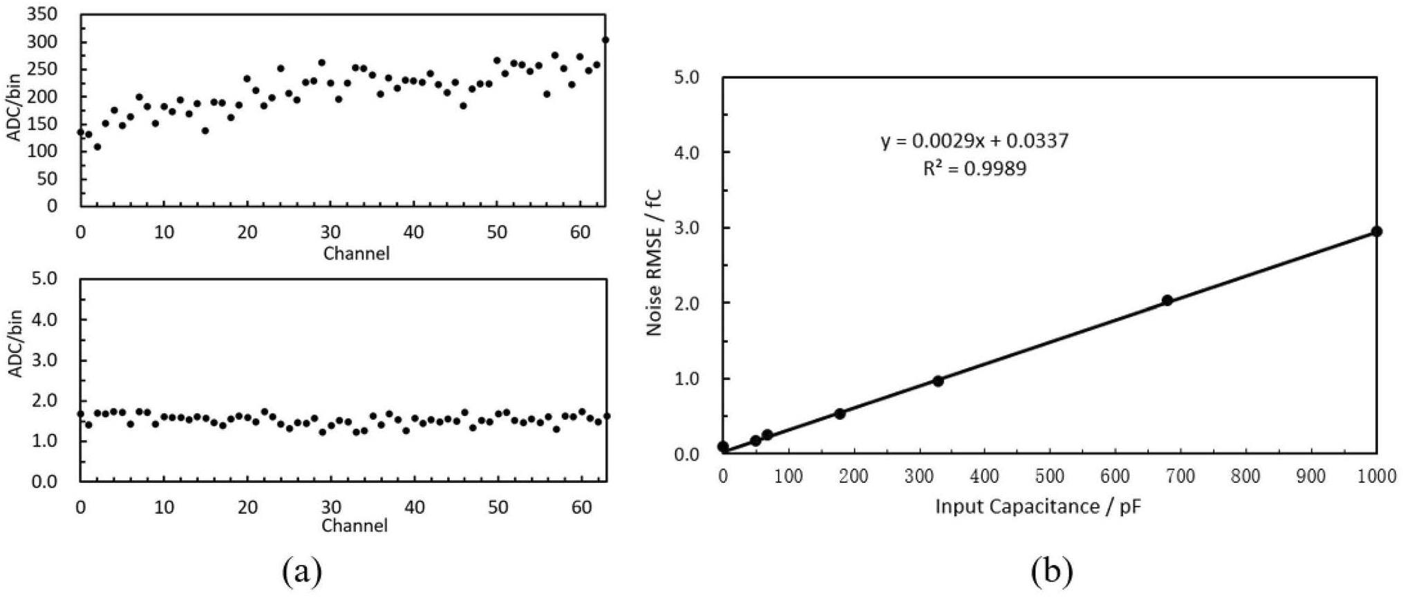
Different load capacitances (0-1000 pF) are mounted between input channel 25 and ground to study the noise level of the readout system under large-area silicon-strip detectors. The noise-slope curve of the IDE1140 is shown in Fig. 5b. The equivalent-noise charge with a capacitive load of 51 pF is 1034 e- (0.166 fC). The input is connected to ground to measure the noise of the 0 pF load. Approximately 10000 events are acquired and the noise is 573 e- (0.092 fC).
Dynamic range and linearity of miniFEE
The chip manual for IDE1140 indicates that the gain in the linear region is 2.6 uA/fC. The gain is set to 0.061 fC/bin by simulating the acquisition circuit in TINA.
As shown in Fig. 6, we perform internal calibration testing of the electronic system in the test mode. The FPGA controls the calibration circuit, as shown in Fig. 4b to inject the specified amplitude voltage-pulse signals into the calibration pin of the IDE1140. These signals are then converted into charge signals using the 2 pF internal-coupling capacitors of the ASIC chip. Approximately 10000 events are acquired and the specific channel internal-calibration results are shown in Fig. 7a. The gain of the internal calibration is 0.062 fC/bin.


As shown in Fig. 6c, we perform external injection testing of the electronic system in the normal mode. A signal generator is used to produce a square wave with an amplitude of 0-100 mV, which is injected into a certain channel. The rising edge of the square wave is used as an external trigger. Based on Fig. 7a, the external injection gain for a certain channel is 0.065 fC/bin.
A comparison of the circuit simulation, internal calibration, and external injection results showed that the electronic system exhibits good linearity in the range of 0-200 fC, and the integral nonlinearity is less than 3%. Furthermore, the relative error of the linear fitting for the three test results is less than 1%.
During testing, we observed that the dynamic range of the ASIC is greater than 200 fC. To test the maximum dynamic range of the ASIC, we modify the gain of the differential-amplification circuit, as shown in Fig. 3b, and perform internal calibration and external injection tests on the three channels using the same testing method, as shown in Fig. 6. The results are presented in Fig. 7b, and the linear range is approximately 0-200 fC, which is consistent with the manual. In the case of ASIC saturation, as the input charge increases, the impedance of the preamplifier increases, leading to a decrease in the gain. The gain decreases when the input charge exceeds 300 fC. After adjustment, the dynamic range is extended to 1200 fC. In future experiments, the dynamic range of the silicon-strip detector readout system may need to be adjusted from 200 fC to a wider range.
CR test of FEE
The readout system was used in the 2022 CERN beam test. The silicon-strip detector designed for the beam test is shown on the left-hand side of Fig. 8. It consists of 400 parallel P+ strips with a thickness of 320 μm. Two hundred readout channels are connected to the silicon strips, and four ASICs are wire-bonded.
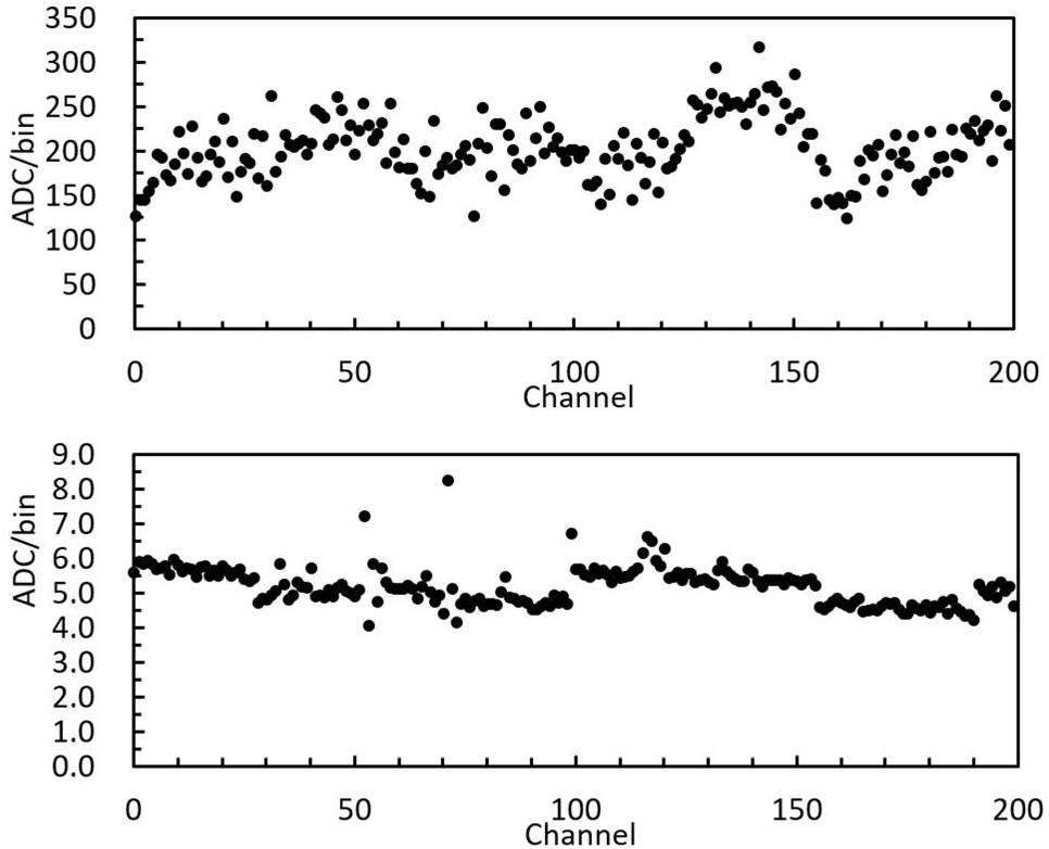
The readout system uses a periodic self-trigger to obtain the pedestal and noise. The test results are presented in Fig. 9. The pedestal values of the channels, with the detector connected, range from 120 to 320 ADC. The RMSE values of the channels are approximately 5.5 ADC (0.341 fC).
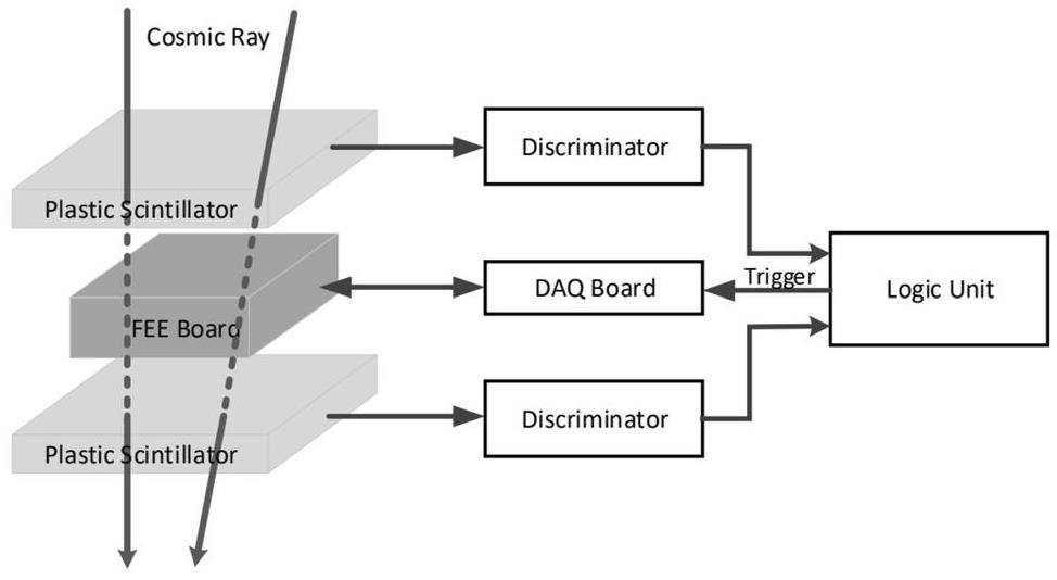
A CR test system is also applied to test the performance of the detector for the MIPs, as shown in Fig. 10. Two plastic scintillators are placed above and below the detector. The size of the plastic scintillators is 12 cm×12 cm×1 cm, which is larger than that of the SCD. Therefore, most of the signals are observed at baseline. The CRs passing through the upper and lower layers of the plastic scintillator are simultaneously used as trigger signals to initiate the data acquisition of the FEE. Theoretically, the energy distribution of CRs follows the Landau distribution. The spectra were fitted to a Landau-convoluted Gaussian function.
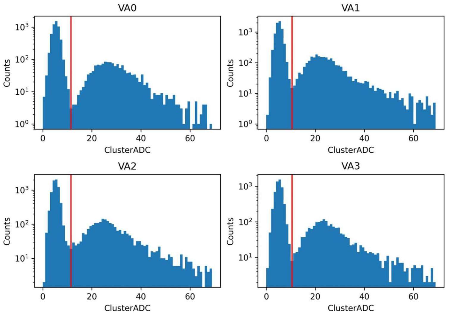
One muon produces the most probable number of 23000 e-h+ pairs in a 320-μm-thick silicon detector. This readout system shows a gain of 15.4 bin/fC, as calculated from a linearity test. Through the analysis of long-term CR-test data, the spectrum can be obtained, as shown in Fig. 11. The red lines in the figure represent the thresholds (at three RMSEs). The most probable parameter of Landau density is located at approximately 33 ADCs. The response uniformity of the four ASICs is good.
Conclusion
This project successfully developed a silicon-strip detector readout system, including the FEE and DAQ. The readout system has 384 channels with a power consumption of 2 W. This detector can simultaneously measure 200 strip channels in the range of 0 fC to 200 fC with 0.341 fC RMS noise. After adjustment, the dynamic range of the readout system can be extended to 1200 fC. In future experiments, the dynamic range may need to be adjusted from 200 fC to a wider range. We have analyzed the beam-test data using a new algorithm, and the charge resolutions of protons and carbon were approximately 0.10 c.u. and 0.20 c.u. on average, respectively, using the novel algorithm [38]. The results indicate that the readout system has low noise and high resolution, satisfying the detection requirements for high-energy CRs.
In future research, we will perform a more detailed energy calibration for the dynamic range of 1200 fC and verify whether this method can be used for charge sharing. In addition, this readout system was designed for beam-test experiments to validate key basic circuits. The next step will be to design a more complex and complete SCD electronic system with more readout channels based on this research.
Overview of the HERD space mission
. Phys. Scr. 97,The space station based detector HERD: precise high energy cosmic rays physics and multimessenger astronomy
. Nucl. Part. Phys. P. 306-308, 85-91 (2019). https://doi.org/10.1016/j.nuclphysbps.2019.07.013Overall status of the high energy cosmic radiation detection facility onboard the Future China's Space Station
.Introduction to the high energy cosmic-radiation detection (HERD) facility onboard China's Future Space Station
.Observation of gravitational waves from a binary black hole merger
. Phys. Rev. Lett. 116,Gravitational waves and gamma-rays from a binary neutron star merger: GW170817 and GRB170817A
. Astrophys. J. Lett. 848,Direct detection of a break in the teraelectronvolt cosmic-ray spectrum of electrons and positrons
. Nature 552, 63-66 (2017). https://doi.org/10.1038/nature24475A novel 3-D calorimeter for the high energy cosmic-radiation detection (HERD) Facility onboard China's Future Space Station
.Study on temperature response of the HERD calorimeter cell
. Radiat. Detect. Technol. Methods 7, 227-233 (2023). https://doi.org/10.1007/s41605-022-00377-7Design and expected performances of the large acceptance calorimeter for the HERD space mission
.Development of the photo-diode subsystem for the HERD calorimeter double-readout
. J. Instrum. 17,FIT: the scintillating fiber tracker of the HERD space mission
.Particle identification capability of Plastic scintillator tiles equipped with SiPMs for the High Energy cosmic Radiation Detection (HERD) facility
. Nucl. Instrum. Methods Phys. Res. Sect. A 983,A preliminary simulation study of influence of backsplash on the plastic scintillator detector design in HERD experiment
. Radiat. Detect. Technol. Methods 5, 332-338 (2021). https://doi.org/10.1007/s41605-021-00245-wCapacitive coupling study of the HERD SCD prototype: preliminary results
. IEEE Trans. Nucl. Sci. 71, 1233-1237 (2024). https://doi.org/10.1109/TNS.2024.3376396Progress of single event effects and hardening technology of CMOS image sensors
. Nucl. Tech. 43,Radiation response characteristics of an embeddable SOI radiation sensor
. Nucl. Tech. 42,Characterization of CIAE developed double-sided silicon strip detector for charged particles
. Nucl. Sci. Tech. 29, 73 (2018). https://doi.org/10.1007/s41365-018-0406-0The tracking system of HERD
.PAMELA silicon tracking system: experience and operation
. Nucl. Instrum. Methods Phys. Res. Sect. A 582, 892-897 (2007). https://doi.org/10.1016/j.nima.2007.07.116The DAMPE silicon–tungsten tracker
. Nucl. Instrum. Methods Phys. Res. Sect. A 831, 378-384 (2016). https://doi.org/10.1016/j.nima.2016.02.077Charge reconstruction of the DAMPE Silicon-Tungsten tracker: A preliminary study with ion beams
. Nucl. Instrum. Methods Phys. Res. Sect. A 886, 48-52 (2018). https://doi.org/10.1016/j.nima.2018.01.007A charge sharing study of silicon microstrip detectors with electrical characterization and SPICE simulation
. Adv. Space Res. 64, 2627-2633 (2019). https://doi.org/10.1016/j.asr.2019.07.005Characterization of silicon microstrip sensors for space astronomy
. Nucl. Sci. Tech. 31, 97 (2020). https://doi.org/10.1007/s41365-020-00811-9Characterization of CIAE developed double-sided silicon strip detector for charged particles
. Nucl. Sci. Tech. 29, 73 (2018). https://doi.org/10.1007/s41365-018-0406-0Signal collection and position reconstruction of silicon strip detectors with 200 µm readout pitch
. Nucl. Instrum. Methods Phys. Res. A 397, 232-242 (1997). https://doi.org/10.1016/S0168-9002(97)00802-4The AGILE silicon tracker: An innovative γ-ray instrument for space
. Nucl. Instrum. Methods Phys. Res. A 501, 280-287 (2003). https://doi.org/10.1016/S0168-9002(02)02047-8Spatial resolution of silicon microstrip detectors
. Nucl. Instrum. Methods Phys. Res. Sect. A 335, 44-58 (1993). https://doi.org/10.1016/0168-9002(93)90255-GOne micron spatial resolution with silicon strip detectors
. Nucl. Instrum. Methods. Phys. Res. Sect. A 348, 485 (1994). https://doi.org/10.1016/0168-9002(94)90785-4Performance of long modules of silicon microstrip detectors
. Nucl. Instrum. Methods Phys. Res. Sect. A 413, 17-30 (1998). https://doi.org/10.1016/S0168-9002(98)00481-1Advances in nuclear detection and readout techniques
. Nucl. Sci. Tech. 34, 20 (2023). https://doi.org/10.1007/s41365-023-01359-0The product information of IDE1140
. https://ideas.no/products/ide1140/Compact 16-channel integrated charge-sensitive preamplifier module for silicon strip detectors
. Nucl. Sci. Tech. 31, 48 (2020). https://doi.org/10.1007/s41365-020-00755-0Design and testing of a miniature silicon strip detector
. Nucl. Sci. Tech. 31, 7 (2019). https://doi.org/10.1007/s41365-019-0714-zANALOG DEVICES., The AD7476
. https://www.analog.com/cn/products/ad7476.htmlDesign of a high-dynamic-range prototype readout system for VLAST calorimeter
. Nucl. Sci. Tech. 34, 149 (2023). https://doi.org/10.1007/s41365-023-01291-3TEXAS INSTRUMENTS., The TLV5638
. https://www.ti.com.cn/product/cn/TLV5638A novel charge reconstruction algorithm applied to the HERD prototype silicon charge detector
. Nucl. Instrum. Methods Phys. Res. Sect. A 1064,The authors declare that they have no competing interests.

