Introduction
The mass of an atom, a fundamental property that inherently connects the atomic and nuclear binding energies, is a unique fingerprint of the atomic nucleus, providing hints on atomic and nuclear structures, as well as the interactions between fundamental particles such as electrons and nuclei, protons, and neutrons [1, 2]. Accurate atomic mass data have significant application value in various physics research fields, including nuclear models, nuclear astrophysics, weak interaction studies, and metrology [1, 3, 4]. In addition, by observing minute deviations from the theory, potential new interactions beyond the standard model (SM) can be probed [5, 6].
Numerous studies have been performed to precisely measure atomic masses using different techniques of mass spectrometry [2]; for example, isochronous mass spectrometry (IMS) [7-10] and Schottky mass spectrometry (SMS) [11, 12] at storage rings, time-of-flight magnetic-rigidity (TOF-Bρ) method [13], multireflection TOF mass spectrometry (MR-TOF-MS) [14], and Penning trap mass spectrometry [15]. Mass spectrometry based on storage rings is a suitable method for the mass measurement of radioactive beams [16-20]. Recently, the CSRe/IMP group installed a double time-of-flight detector system to improve the measurement accuracy to below 10-6 [18, 21, 22] and precisely determined the masses of a few neutron-deficient nuclei [23-26] for nuclear structure and astrophysics interest. The MR-ToF method was implemented at the GSI [27] RIKEN [28] and TITAN [29] aim to measure short-lived nuclei with resolution powers greater thatn 105 and flight times shorter than a few milliseconds.
Penning trap mass spectrometry is considered the most precise measurement method for atomic mass owing to its extremely high accuracy at 10-9 or below. Using a novel phase-imaging ion cyclotron resonance (PI-ICR) technique developed by Eliseev et al. [30], the SHIPTRAP group reported the precise measurement of superheavy element masses [31]. Similar techniques have also been implemented in other online Penning trap facilities, such as JYFLTRAP [32] and TITAN [33] for the measurement of short-lived nuclei. For long-lived or stable species, the precision achievable by Penning-trap mass spectrometry is even higher, up to 10-11, using the Fourier-transform ion cyclotron resonance (FT-ICR) technique. The higher accuracy is simply due to the longer measurement times required for stable nuclei, because the measurement precision is inversely proportional to the observation time
FT-ICR is a non-destructive measurement technique capable of detecting single ions in Penning traps. The ions oscillating in the electromagnetic field can induce image currents in the trap electrodes, which are typically a few fA and have frequency features identical to the eigenmotions of the ions. In 1992, Jefferts et al. [37] described the development of a detection system consisting of a superconducting inductor and a GaAs field-effect transistor preamplifier for image current-signal readout. Subsequently, Ulmer et al. [38] presented an optimization procedure for a helical superconducting resonator, whereas Nagahama et al. [39] reported another design for a toroidal resonator with extremely high quality factors. Currently, this detection system is indispensable for precision Penning-trap mass spectrometry based on the FT-ICR method [40].
A new cryogenic Penning trap set-up is currently under construction in Shanghai, China. The goal of this Penning trap is to detect the decay of long-lived electronic metastable states in a single ion confined within the trap directly, such as
Principle of Penning Trap
Ion motion in a penning trap
In a homogeneous magnetic field, a charged particle with mass m and charge q experiences a Lorentz force
The presence of an electrostatic quadrupolar field modifies the pure cyclotron motion of an ion in the magnetic field, resulting in three independent eigen motions with frequencies
Principle of image charge detection
The frequency of motion of a single ion is determined through the utilization of the FT-ICR technique. The detection principle is illustrated in Fig. 1. The oscillating charged particles induce an image current in the trap electrodes. With a large impedance, this small current signal is converted into a detectable voltage. This impedance is realized by a superconducting inductor L connected in parallel to the trap, forming a tank circuit with parasitic capacitance Cp and a resonance frequency νres

Cryogenic electronic detection system development
Cryogenic Amplifiers
The detection system comprises two crucial components: a high-Q resonator and cryogenic low-noise amplifier. The ion signal from the trap can be affected by noise as it travels through the transmission line, which is several meters long. Therefore, using a low-noise amplifier positioned in the cryogenic region, close to the downstream of the resonator, is essential for signal amplification. Currently, most commercial amplifiers with a bandwidth that meets the ion frequencies in Penning traps cannot operate at liquid helium temperatures because the charge carriers in standard silicon semiconductors can freeze. In addition, some amplifiers suffer from high power consumption and significant input noise, rendering them unsuitable for very weak image charge signals. A desirable amplifier requires low noise and power consumption, along with a suitable bandwidth in the range of a few hundred kHz to tens of MHz.
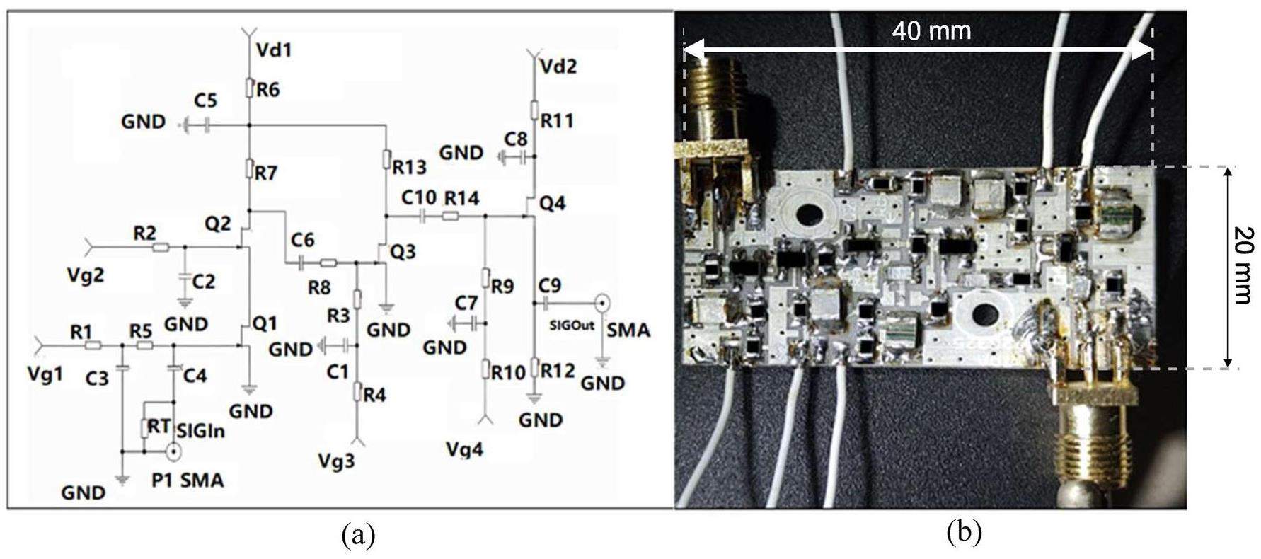
The first low-noise cryogenic amplifier design, denoted AMP1 is shown in Fig. 2, where the core component, a GaAs based field effect transistor (MESFET), was tested with excellent performance at cryogenic temperatures. In this design, the first stage comprised a cascode common-source amplifier with two FETs to mitigate the Miller effect. This significantly reduces the amplifier’s back-action on the resonator’s quality factor caused by the parasitic Miller capacitance. The second stage is a standard common-source amplifier connected to the output of the first stage for additional amplification. The third stage, which is also called a source follower, does not amplify the signal but rather aims for impedance matching. The entire fabrication process utilized a printed circuit board (PCB) technique, with a polytetrafluoroethylene (PTFE) substrate to minimize dielectric loss. All electronic components, including FETs denoted here as Q1 to Q4, resistors, and capacitors, are surface-mountable, resulting in an amplifier board with dimensions 20 mm × 40 mm and 1.5 mm in thickness. We used metal film resistors and stacked metallized film chip capacitors with a low-temperature drift. Note that all the FETs used in this study were dual-gate GaAs transistors. However, we shortened the two gates Q1 and Q2 in the cascode stage to increase the channel length and thus reduce the 1/f-noise of the transistor in the low-frequency range. Another FET, referred to as Q5, was placed on the PCB board (not shown in the design sheet). The dual-gate FET aims to replace the cascode stage for comparison. The signal input and output were coupled via SMA connectors. The four FETs on the PCB board were operated with a total of six bias voltages, denoted here as Vg1, Vg2, and Vd1 for cascode stage gates and drain voltages, Vg3 and Vd1 for the second-stage gate and drain voltages, and Vg4 and Vd2 for the source-follower gate and drain voltages. In practice, Vg1 and Vg3 control the opening of the first and second stages, respectively, whereas Vg2 and Vg4 are grounded to reduce the number of voltage supply channels. The first and second stages share the same drain voltage, whereas a separate drain voltage supplied to the third stage can reduce power consumption. Consequently, the resulting total power consumption of the amplifier was approximately 6 m watts.
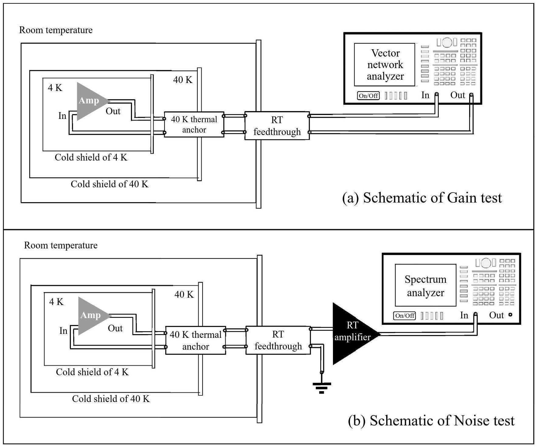
The gain and noise features of the amplifier are mainly determined by the FETs, and the first transistor (Q1) among the four FETs on the PCB board has the most significant impact on the input noise. In this study, we evaluate the performance of a low-noise amplifier using various FETs placed at Q1. The measurements were performed at the cold-head base 4 K cryogenic stage. A transmission network was established to measure the amplifier gain, as shown in Fig. 3(a). A vector network analyzer was used to deliver and receive the RF signal. The input voltage noise of the amplifier was measured using a spectrum analyzer, which included an additional RT amplifier with a known gain in the network, as shown in Fig. 3(b). The cryogenic amplifier input is then grounded. The noise spectrum measured by the spectrum analyzer has the following form:
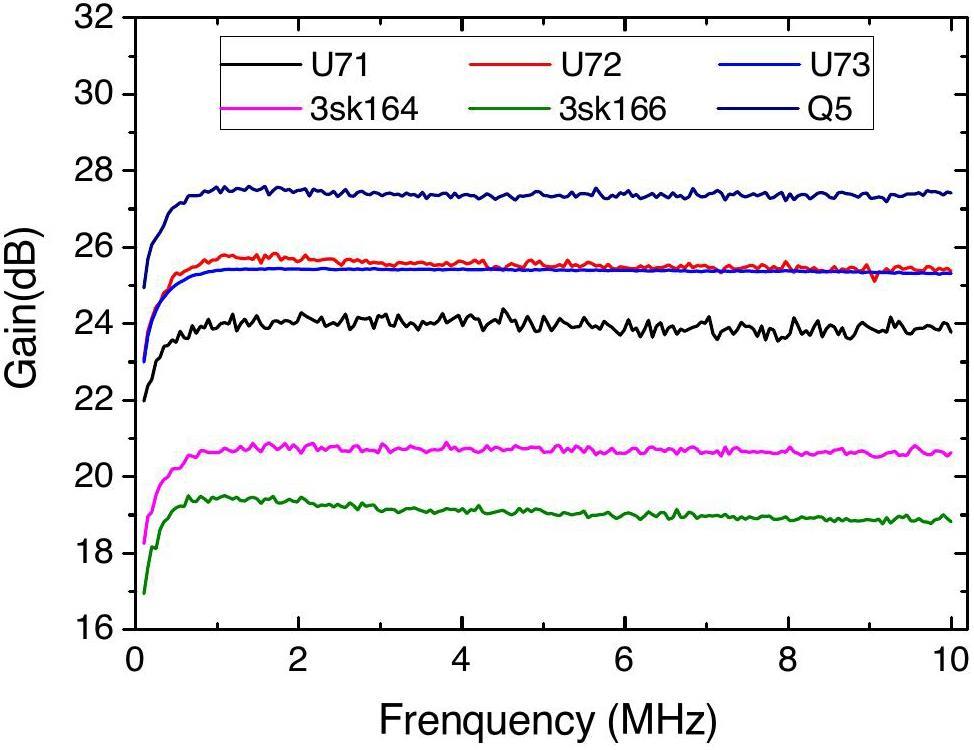
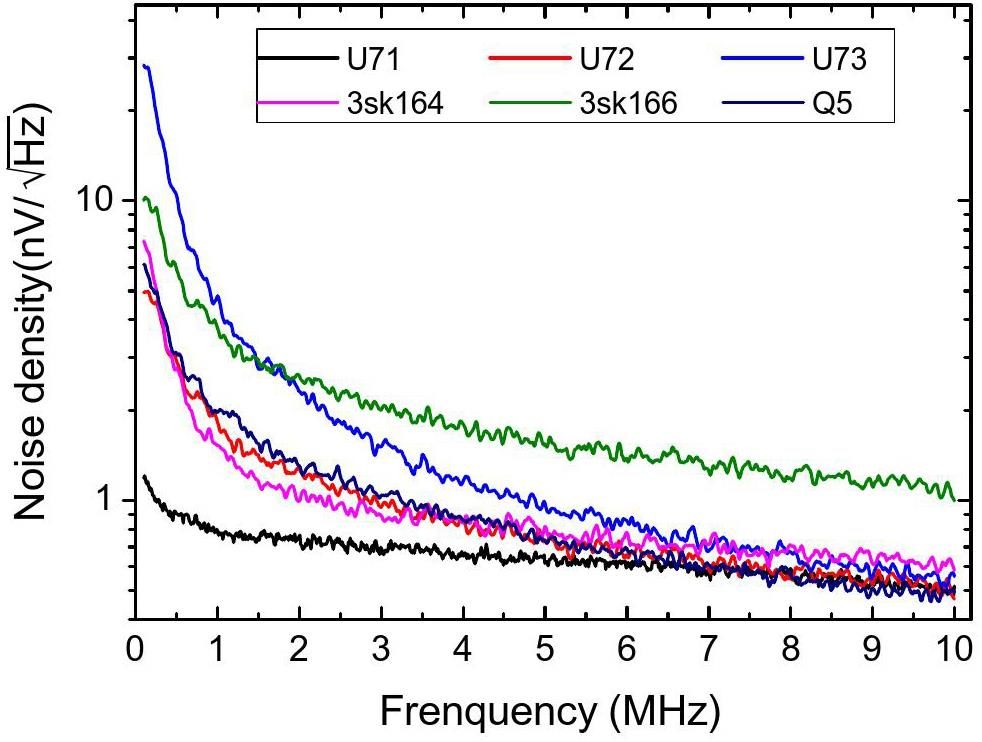
The measured forward transmission S21 and input voltage noise of the cryogenic amplifier with different first FETs at Q1 are shown in Fig. 4 and Fig. 5, respectively. The remaining components remain unchanged. Q2, Q3 and Q4 are CF739, Ne25139-U71 and CF739, respectively. For each FET, the gate voltage of each FET is tuned to the working point. In general, the amplifier with Ne25139 series at Q1 exhibited a higher amplification factor than those with 3sk164 and 3sk166 in the frequency range of 0.1 10 MHz. The input voltage noise of the amplifier, which consists of 1/f noise and white noise, is dominant by the noise of Q1. To detect the axial frequency of the ion in the Penning trap, input noise within the frequency range of a few hundred kilohertz to 1 MHz is critical. The voltage noise densities of the FETs are summarized in Table 1. Ne25139-U71 demonstrates the lowest 1/f noise, whereas the noise levels of Ne25139-U73 and 3sk166 are the highest. Notably, the measured input noise could contain noise from the transmission line because we ground the input of the amplifier at RT feedthrough. However, we did not observe any significant effect on the voltage noise density measurement.
| FET(Q1) | Noise ( |
Idss (mA) |
|---|---|---|
| Ne25139-U71 | 0.8 | 5-15 |
| Ne25139-U72 | 1.8 | 10-25 |
| Ne25139-U73 | 4.8 | 20-35 |
| sk164 | 1.5 | 10-35 |
| sk166 | 3.7 | 20-80 |
| Ne25139-U71 wo. cas. (Q5) | 1.9 | 5-15 |
At a sufficiently low temperature, the fluctuation of the carrier mobility owing to the random scattering of impurities dominates the 1/f noise. This process can be described using the empirical Hooge equation
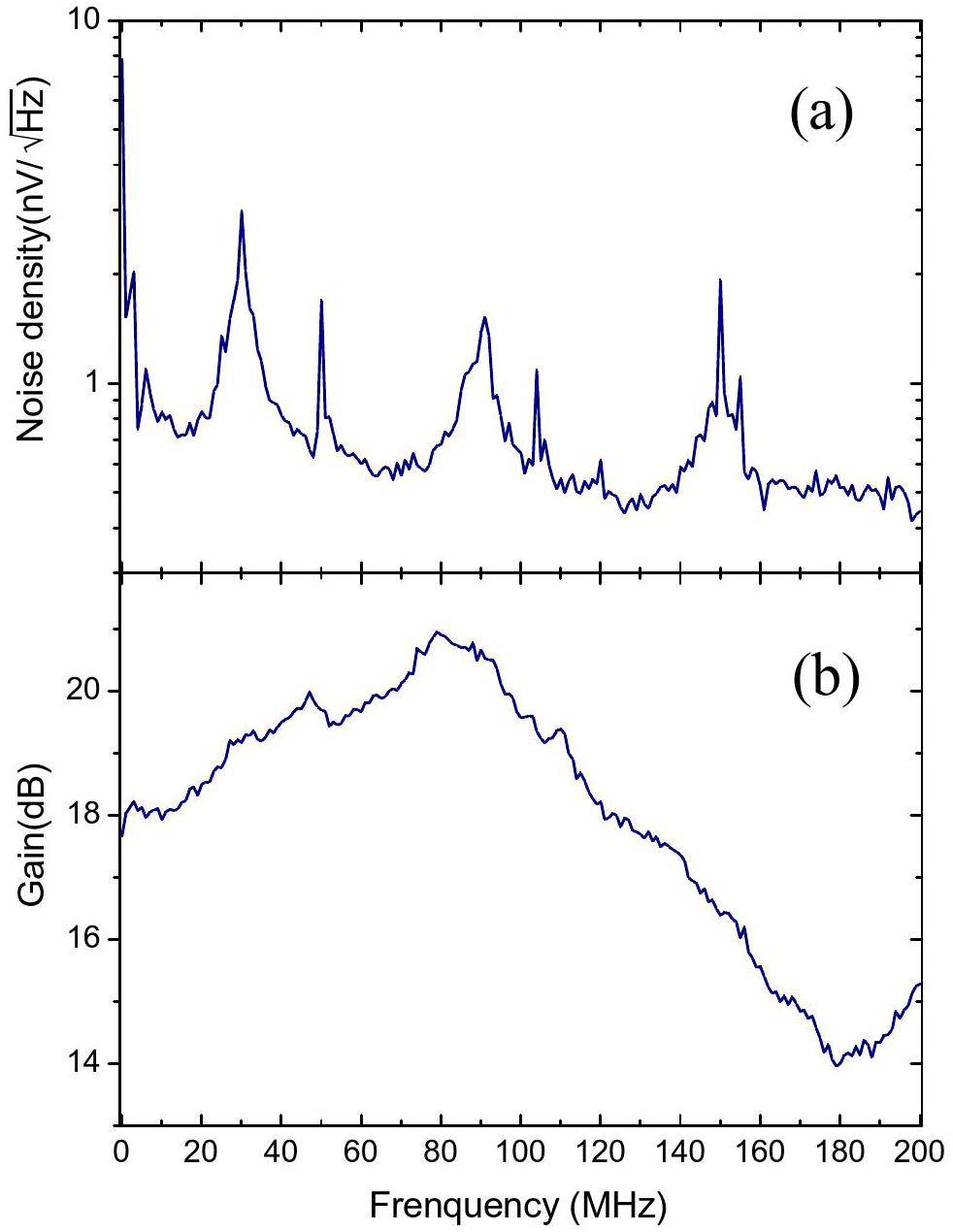
AMP1 was designed for an axial frequency readout and had the highest gain in the relevant frequency range. However, the frequency of the cyclotron is not within this range. Although the cyclotron frequency is usually read out through sideband coupling, which couples the radial motion to the axial motion of the ion, it is also beneficial to directly detect the cyclotron motion using a cryogenic amplifier specifically designed for that frequency range. For this purpose, we developed another cryogenic amplifier, denoted here as AMP2, which is similar to AMP1 but excludes the second common-source amplification stage. The cascode stage comprises two ATF35143 transistors. The measured gain and input voltage noise of AMP2 in the 1–200 MHz frequency range are shown in Fig. 6. At the highest frequency, the amplifier still has a gain of 15 dB. Note that noise peaks in the high-frequency range may originate from the environment.
Resonator
The other component of the cryogenic detection system can be described as an effective parallel RLC-circuit, in experimental realization, manufactured with a solenoidal coil wound on a PTFE core and mounted in a cylindrical housing. The Q value of the tank circuit was strongly influenced by the series resistance and self-capacitance of the coil. Both the ohmic and dielectric losses should be minimized to achieve a high equivalent parallel resistance. Close to the resonance frequency, Rp can be approximated in terms of the capacitor’s equivalent series resistance (ESR1) and the equivalent winding resistance of the inductor, RL:
A resonator wound with superconducting NbTi wires can minimize the conductive loss when operated below the critical temperature of
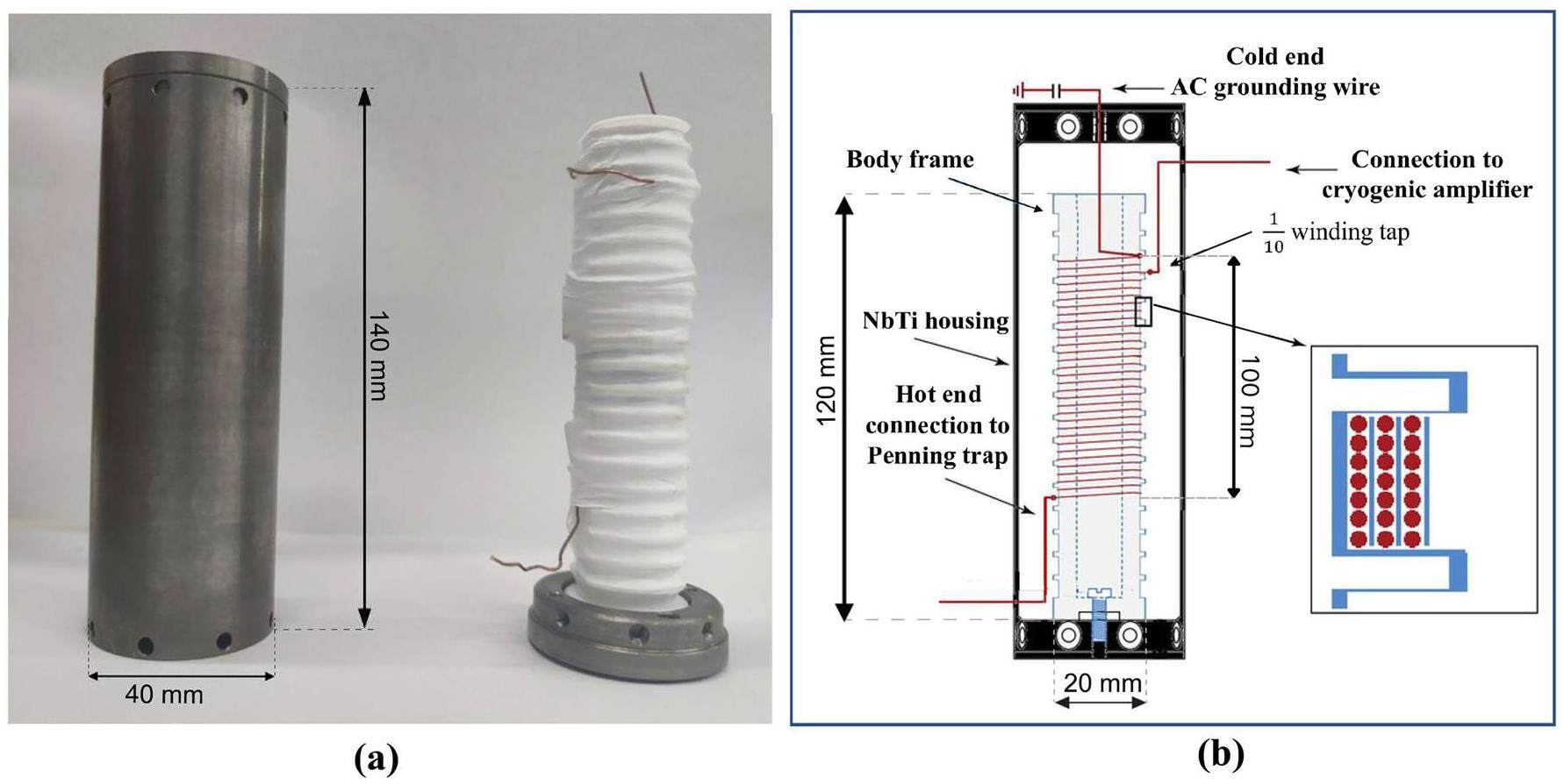
Ensuring good heat contact between the wire and PTFE core is crucial because at the phase transition to the superconducting state, electrons condense to the BCS ground state, leading to a decrease in the heat conduction coefficient of NbTi. The windings were fixed to the body frame using PTFE thread-seal tape, and the body was pressed against the bottom plate of the housing using a brass screw. This configuration also ensured mechanical stability of the coil during thermal cycling. Both ends of the coil were soldered to high-conductivity copper wires with 0.7 mm diameters. One end was designed to connect to the trap, namely the “hot end,” whereas the other was RF grounded, denoted here as the “cold end.” A 1/10 winding tap was present in the coil, where the signal was picked up and fed into the input of the cryogenic amplifier. This design utilized the coil as a self-transformer, effectively reducing the noise from subsequent electronics to the trap.
The measurement setup is illustrated in Fig. 8(a). The thermal noise of the resonator was amplified by the cryogenic amplifier mentioned above as well as an RT amplifier before entering the spectrum analyzer. The measured noise spectra are presented in Figs. 8(b). To estimate the values rapidly, the Q value of the resonator can be determined from the ratio of the resonance frequency vres to the width at the -3 dB point below the resonance peak. A more accurate result is obtained by fitting a line-shaped model of the resonator impedance to the experimentally obtained data.

To determine the inductance and self-capacitance of the coil, we soldered an additional capacitor parallel to it, which shifted the resonance frequency to
Summary
A cryogenic electronic system for image charge detection was developed for use in the Shanghai Penning Trap. The system comprises two primary components: a cryogenic amplifier with low noise and high gain and a helical superconducting resonator, which resonantly amplifies the image current of a single ion. This system enables the detection of minute signals from ions, facilitating further amplification and spectral analysis at RT. Low-noise cryogenic amplifiers were engineered in three amplification stages. The initial stage employs a cascode common-source amplifier with two FETs to mitigate the Miller effect. The second stage adopts another common-source design for cascaded amplification, whereas the third stage employs a source follower to ensure impedance matching. The input voltage noise and amplification factors of the amplifiers were measured at the cryogenic stage using various FETs employed at the first transistor position. In the frequency range of 0.1∼10 MHz, the highest gain measured was greater than 27 dB for Ne25139-U73, whereas Ne25139-U71 exhibited the lowest 1/f noise. Additionally, we observed a correlation between 1/f noise and the saturated drain-source current in FETs. By shortening the two gates of Ne25139-U71 to increase the channel length, we also achieved a reduction in 1/f noise. To detect the cyclotron motion of the ion directly, we developed another amplifier that can be operated in the frequency range of 1 MHz to 200 MHz, demonstrating an amplification factor exceeding 15 dB at the highest frequency. The helical resonator, which was fabricated with 900 turns of NbTi superconducting wires in three layers, was housed in a cylindrical NbTi enclosure. After the measurements at the cold-head base cryogenic stage, the inductance, self-capacitance, and resonance frequency were determined. The unloaded Q value is 98004. The loss in the coil arises from several factors, including soldering at the NbTi-to-Cu joint and the dielectric loss within the coil. By enhancing the joint contact with a spot welder or high indium solder and ensuring good thermal contact between the wire solder joints and the PTFE core, a lower series resistive loss can be achieved. Additionally, using a thicker insulator for the NbTi wire to increase the spacing between the wires further reduces the dielectric loss, thereby increasing the Q value.
High-accuracy mass spectrometry with stored ions
. Phys. Rep. 425, 1-78 (2006). https://doi.org/10.1016/j.physrep.2005.10.011Masses of exotic nuclei
. Prog. Part. Nucl. Phys. 120,The AME 2020 atomic mass evaluation (I). Evaluation of input data, and adjustment procedures*
. Chinese Phys. C 45,The AME 2020 atomic mass evaluation (II). Tables, graphs and references*
. Chinese Phys. C 45,Probing New Long-Range Interactions by Isotope Shift Spectroscopy
. Phys. Rev. Lett. 120,Observation of Nonlinearity of Generalized King Plot in the Search for New Boson
. Phys. Rev. X 12,First isochronous mass measurements with two time-of-flight detectors at CSRe
. Phys. Scr. 2015,Precision mass measurements of short-lived nuclides at HIRFL-CSR in Lanzhou
. Front. Phys. 13,Charge resolution in the isochronous mass spectrometry and the mass of 51Co
. Nucl. Sci. Tech. 32, 37 (2021). https://doi.org/10.1007/s41365-021-00876-0Isochronous mass measurements of Tz=−1 fp-shell nuclei from projectile fragmentation of 58Ni
. Phys. Rev. C 98,Heavy-ion storage rings and their use in precision experiments with highly charged ions
. Part. Nucl. Phys. 115,First application of combined isochronous and Schottky mass spectrometry: Half-lives of fully ionized 49Cr24+ and 53Fe26+ atoms
. Phys. Rev. C 97,Mapping the frontiers of the nuclear mass surface
. J. Phys. Conf. Ser 1668,Multiple-reflection time-of-flight mass spectrometry
. Int. J. Mass Spectrom. 349, 134-144 (2013). https://doi.org/10.1016/j.ijms.2013.06.005Penning-trap mass measurements in atomic and nuclear physics
. Annu. Rev. Nucl. Part. Sci. 68, 45-74 (2018). https://doi.org/10.1146/annurev-nucl-102711-094939Mass measurement of cooled neutron-deficient bismuth projectile fragments with time-resolved Schottky mass spectrometry at the FRS-ESR facility
. Nucl. Phys. A 756, 3-38 (2005). https://doi.org/10.1016/j.nuclphysa.2005.03.015Masses of ground and isomeric states of 101In and configuration-dependent shell evolution in odd-A indium isotopes
. Phys. Rev. C 100,Characterization of a double Time-Of-Flight detector system for accurate velocity measurement in a storage ring using laser beams
. Nucl. Instrum. Methods Phys. Res. Sect. A-Accel. Spectrom. Dect. Assoc. Equ. 931, 52-59 (2019). https://doi.org/10.1016/j.nima.2019.03.058First Application of Mass Measurements with the Rare-RI Ring Reveals the Solar r-Process Abundance Trend at A=122 and A=123
. Phys. Rev. Lett. 128,First Application of Mass Measurements with the Rare-RI Ring Reveals the Solar r-Process Abundance Trend at A=122 and A=123
. J. Phys. Conf. Ser. 1643,Mass Measurement of Short-lived Nuclei at HIRFL-CSR
. EPJ Web Conf. 66, 02107 (2014). https://doi.org/10.1051/epjconf/20146602107Mass measurements for the Tz=−2 fp-shell nuclei 40Ti, 44Cr, 46Mn, 48Fe, 50Co, and 52Ni
. Phys. Rev. C 102,Isochronous mass measurements of neutron-deficient nuclei from 112Sn projectile fragmentation
. Phys. Rev. C 107,Mass Measurement of Upper fp-Shell N = Z- 2 and N = Z- 1 Nuclei and the Importance of Three-Nucleon Force along the N = Z Line
. Phys. Rev. Lett. 130,Mass measurements show slowdown of rapid proton capture process at waiting-point nucleus 64Ge
. Nat. Phys. 19, 1091-1097 (2023). https://doi.org/10.1038/s41567-023-02034-2Mass measurements of neutron-deficient Y, Zr, and Nb isotopes and their impact on rp and vp nucleosynthesis processes
. Phys. Lett. B 781, 358-363 (2018). https://doi.org/10.1016/j.physletb.2018.04.009A high-performance multiple-reflection time-of-flight mass spectrometer and isobar separator for the research with exotic nuclei
. Nucl. Instrum. Methods Phys. Res. Sect. A-Accel. Spectrom. Dect. Assoc. Equ. 777, 172-188 (2015). https://doi.org/10.1016/j.nima.2014.12.094First online multireflection time-of-flight mass measurements of isobar chains produced by fusion-evaporation reactions: Toward identification of superheavy elements via mass spectroscopy
. Phys. Rev. C 95,Mass measurements of 60-63Ga reduce x-ray burst model uncertainties and extend the evaluated T= 1isobaric multiplet mass equation
. Phys. Rev. C 104,Phase-imaging ion-cyclotron-resonance measurements for short-lived nuclides
. Phys. Rev. Lett. 110,Direct high-precision mass spectrometry of superheavy elements with SHIPTRAP
. Phys. Rev. C 106,Phase-Imaging Ion-Cyclotron-Resonance technique at the JYFLTRAP double Penning trap mass spectrometer
. Eur. Phys. J. A 54, 154 (2018). https://doi.org/10.1140/epja/i2018-12589-yTowards high precision mass measurements of Highly Charged Ions using the Phase-Imaging Ion-Cyclotron-Resonance technique at TITAN
. Hyperfine Interact. 241, 37 (2020). https://doi.org/10.1007/s10751-020-1705-5High-precision measurement of the atomic mass of the electron
. Nature 506, 467-470 (2014). https://doi.org/10.1038/nature13026High-precision measurement of the proton’s atomic mass
. Phys. Rev. Lett. 113,A 16-parts-per-trillion measurement of the antiproton-to-proton charge–mass ratio
. Nature 601, 53-57 (2022). https://doi.org/10.1038/s41586-021-04203-wSuperconducting resonator and a cryogenic GaAs field-effect transistor amplifier as a single-ion detection system
. Rev. Sci. Instrum. 64, 737-740 (1993). https://doi.org/10.1063/1.1144153The quality factor of a superconducting rf resonator in a magnetic field
. Rev. Sci. Instrum. 80, 12 (2009). https://doi.org/10.1063/1.3271537Highly sensitive superconducting circuits at 700 kHz with tunable quality factors for image-current detection of single trapped antiprotons
. Rev. Sci. Instrum. 87, 11 (2016). https://doi.org/10.1063/1.4967493The ALPHATRAP experiment
. Eur. Phys. J. Spec. Top. 227, 1425-1491 (2019). https://doi.org/10.1140/epjst/e2018-800225-2Experimental access to observing decay from extremely long-lived metastable electronic states via Penning trap spectrometry
. Phys. Rev. Res. 5,Geonium theory: Physics of a single electron or ion in a Penning trap
. Rev. Mod. Phys. 58, 233 (1986). https://doi.org/10.1103/RevModPhys.58.233Precision spectroscopy of a charged particle in an imperfect Penning trap
. Phys. Rev. A 25, 2423 (1982). https://doi.org/10.1103/PhysRevA.25.2423Eddy current losses in transformer windings and circuit wiring
. 1988.p. R2-1,The authors declare that they have no competing interests.
The ESR incorporates the capacitor’s dielectric and conduction losses. The losses due to electromagnetic radiation of the tuned circuit were neglected.

