Introduction
The Cooling Storage Ring (CSR) [1-3] of the Heavy Ion Research Facility in Lanzhou (HIRFL) is a powerful machine developed to probe uncharted fields of nuclear physics, delivering a variety of heavy ions of elements from hydrogen to uranium with energies up to 1 GeV/u. The external-target experiment (CEE) [4] at the HIRFL-CSR, which is designed to study the nuclear matter phase structure at low temperatures and high baryon densities [5], is currently under development. The design specifications of the CEE include a detection beam energy ranging from 0.3 GeV/u to 2.8 GeV/u, a maximum collision system of uranium+uranium, and a maximum event rate of 104 s-1, corresponding to a maximum beam particle rate of approximately 106 s-1 [4]. As shown in Fig. 1, the CEE detector consists of a dipole magnet, a beam monitor [6-10], a start time detector (T0) [11, 12], a time projection chamber (TPC) [13-16], an inner time-of-flight detector (iTOF) [17, 18], multi-wire drift chambers (MWDCs) [19-21], an external time-of-flight detector (eTOF) [22, 23], and a zero-degree calorimeter (ZDC) [24-26].
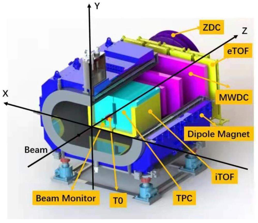
The beam monitor of the CEE spectrometer is designed to monitor the beam status and improve the reconstruction resolution of the primary vertex, which is otherwise determined by the TPC and MWDCs. The main specifications include a spatial resolution of less than 50 μm and a time resolution of less than 1 μs. To achieve these specifications, custom-designed pixel chips named Topmetal-CEEv1 [27], which can simultaneously measure amplitude and time, are deployed in the detector. This approach combines the functions of a charge sensor and readout application-specific integrated circuit (ASIC).
To configure the pixel chips and communicate with the data acquisition system (DAQ) [28-31], trigger [32, 33] and clock systems [34, 35], an electronic system was developed.
To simultaneously accommodate the requirements regarding the spatial resolution and beam particle rate, a medium pixel pitch size of approximately 100 μm combined with amplitude measurement is desired. For the beam particle rate requirement, the shaping time of the pixel analog front end needs must be as short as approximately 0.5 μs. For the time resolution requirement, a coarse time measurement scheme with precision equal to the system clock cycle is sufficient. The required readout speed depends on the number of pixels fired by each beam particle. In a typical case, it is approximately 2.88 Gbps, assuming that all data (not only triggered events) are read out.
This paper mainly presents the detailed design of the entire readout electronics of the beam monitor, as well as its performance in terms of basic electronic functionality and responses to α particles and heavy-ion beams.
Architecture of the readout electronics
As shown in Fig. 2, the readout electronics system of the beam monitor mainly consists of two bonding boards, each of which carries four Topmetal-CEEv1 chips, two front-end cards (FECs), one readout and control unit (RCU), a commercial power module, one DAQ board, one master trigger module (MTM), one slave trigger module (STM), one master clock module (MCM), and one slave clock module (SCM). The power module is used to supply power to the RCU, STM, and SCM through the backplane of the crate. The MTM and STM are designed to generate trigger signals for valid data readout [33], whereas the MCM and SCM are designed to provide high-quality synchronous clocks for all subdetectors [35]. The DAQ board is used for data transfer and command transfer. The bonding board, FEC, and RCU are specifically designed for the beam monitor, whereas the others are common modules provided by the DAQ, trigger, and clock systems of the CEE.
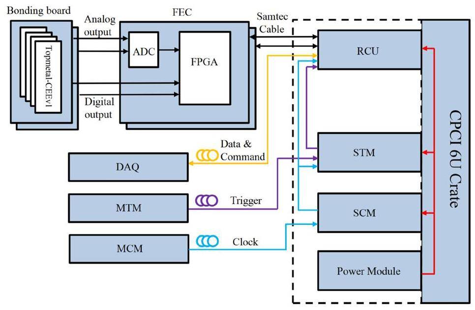
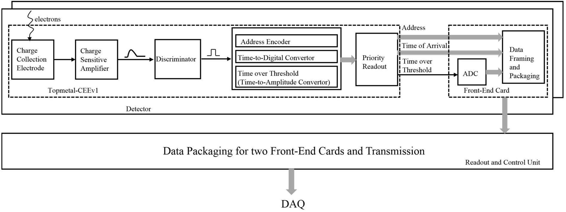
The signal processing chain of the beam monitor is shown in Fig. 3. The charge-collection electrodes of the pixels of the Topmetal-CEEv1 chip detect electrons generated by particle ionization in the gas. The data are arranged into frames that are further packaged in two FECs, then combined in the RCU before being sent to the DAQ of the CEE. Each fired pixel has digital and analog outputs. The analog outputs are digitized using an analog-to-digital converter (ADC) [36, 37] on the FEC. The data are packed using a field-programmable gate array (FPGA) and then transferred to the RCU via a high-speed SAMTEC cable with a length of 10 m. The RCU receives and packs the data from two directions according to the frame format required by the DAQ.
Front-end electronics
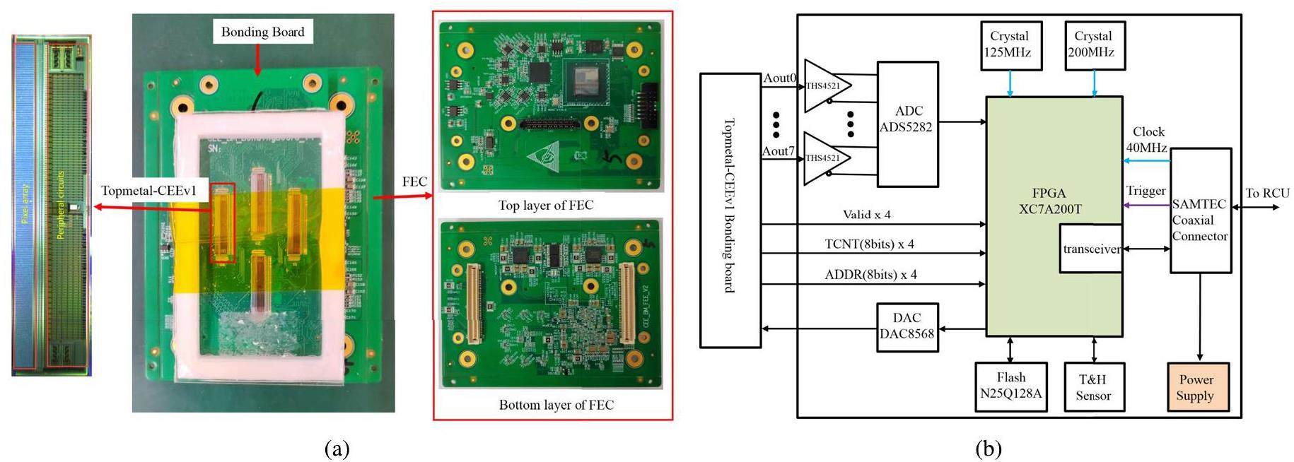
As shown in Fig. 4a, the front-end electronics (FEE) consist of a bonding board carrying the Topmetal-CEEv1 chips, and an FEC. These have a daughterboard and motherboard structure. Because the beam monitor is placed inside a magnetic shield in the dipole magnet, the size of the electronics is constrained.
Topmetal-CEEv1 chip
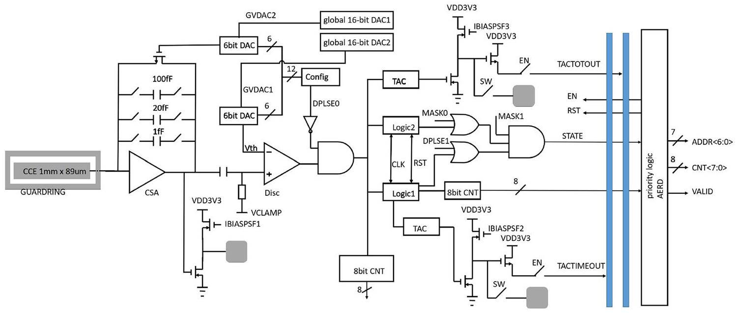
The Topmetal-CEEv1 chips shown in Fig. 4a are placed in the frontmost position of the entire readout electronics system. They collect charges and amplify and digitize signals. The die size of each chip is 4.2 mm×19 mm. Each chip is composed of 180 channels with a pitch of 100 μm and peripheral circuits. The structure of the channels is shown in Fig. 5. Each channel consists of a charge-collection electrode (CCE), charge-sensitive amplifier (CSA), discriminator, time-to-amplitude converter, and logic circuit. The CCE is the topmost exposed metal with a size of 1 mm×89 μm. The peak time of the CSA is approximately 100 ns, and the shaping time is tunable from 0.5 μs to 2 ms. Each channel achieves amplitude measurement through the time-over-threshold (TOT) [38] method and address encoding. The data-driven readout scheme [39, 40] is adopted in Topmetal-CEEv1 to improve the effective readout speed. The 180 channels are divided into two subgroups. Each subgroup individually employs priority logic and only channels with hits are read out. Each subgroup outputs 7-bit channel addresses, 8-bit counters for time measurements, and analog TOT amplitudes. The detailed design and characterization of the Topmetal-CEEv1 chip have been published in Ref. [27].
To demonstrate the needs of a new chip in the Topmetal chip series, the main features of Topmetal-CEEv1 are shown in Table 1, with the preexisting Topmetal-II- [41, 42] and Topmetal-M [43] chips for comparison. To accommodate a maximum beam particle rate of approximately 106 s-1, one-column pixels with a large CCE size and the data-driven readout scheme are adopted in the Topmetal-CEEv1 chip.
| Topmetal-CEEv1 | Topmetal-II- | Topmetal-M | |
|---|---|---|---|
| Chip area | 4.2 mm×19 mm | 8 mm×9 mm | 18 mm×23 mm |
| Number of pixels | 1 × 180 | 72 × 72 | 400 × 512 |
| Pixel pitch | 100 μm | 83 μm | 40 μm |
| CCE size | 1 mm×89 μm | 25 μm×25 μm | 25 μm×25 μm |
| Readout scheme | Data-driven | Rolling-shutter | Rolling-shutter |
| Readout rate | 40 MPixels/s | 4.6 kFrames/s | 1.6 kFrames/s |
| Amplitude meas. | Yes | Yes | Yes |
| Time meas. | Yes | No | Yes |
Bonding board design
The bonding board is used for chip gluing and wire bonding, as shown in Fig. 4a. Four Topmetal-CEEv1 chips are arranged in three rows on the top side of the board. Two chips are placed in the middle row to satisfy the requirements of the detection area. Two other chips are placed in the other rows to further improve the position resolution. Considering the influence of radiation, only resistors and capacitors are placed on the rear side of the board. Two high-density connectors are used to lead out signals from the bonding board, and sufficient power pins are reserved on these connectors for the chip power supply.
Front-end card design
Hardware
The FEC, based on the Xilinx Artix-7 FPGA XC7A200T, is designed to provide the required power, configure the Topmetal-CEEv1 chip, convert the analog signals, pack data, and transfer them to the RCU. Figure 4 shows a photograph of the FEE and a block diagram of the FEC. Each Topmetal-CEEv1 chip has two single-ended analog outputs. Each output is fed into a fully differential operational amplifier, which is used to adjust the amplitude and bias of the signal to satisfy the input requirements of the ADC. The differential analog outputs are then digitized using an off-chip 8-channel ADC. The digitized outputs, together with the digital outputs of the chip, are sent to the FPGA. After framing and packaging, the data are transmitted to the RCU via a high-speed transceiver inside the FPGA. An 8-channel 16-bit DAC provides the bias voltages for four Topmetal-CEEv1 chips. Two crystal oscillators are present on the board. A 125 MHz oscillator is used as the transceiver, whereas a 200 MHz oscillator is used as the local system clock. A 128 Mb SPI flash is used to store the firmware logic. Temperature and humidity sensors are deployed onboard to monitor the status of the environment. The connector between the FEC and RCU is a SAMTEC coaxial cable used for power, data, trigger, and clock transmissions.
The front-end electronics are powered from the back end through the 10-meter SAMTEC coaxial cable. Several aspects have been considered in the power supply design to reduce the voltage drop on the ground of the FEC. First, except for essential signal pins, all other pins of the cable are used for power. Second, the input voltage is set as high as possible to reduce the total current. Third, high-efficiency DC-DC converters are used.
The overall input power supply voltage of the FEC is 10 V. Two quad-output power modules MPM54304 in an ultrathin package are adopted to generate power for the digital circuits of Topmetal-CEEv1, FPGA, and the other chips on the board. Three ADP7158 low-noise low-dropout linear regulators (LDOs) are used to power the ADC and analog circuits of Topmetal-CEEv1. During the test, the static current of the front-end electronics is approximately 0.5 A, resulting in a voltage drop of several tens of millivolts on the ground, which has no impact on signal transmission.
Firmware
As shown in Fig. 6, the FEC logic mainly consists of four parts: control logic, data processing logic, clock and synchronization logic, and transmission logic.
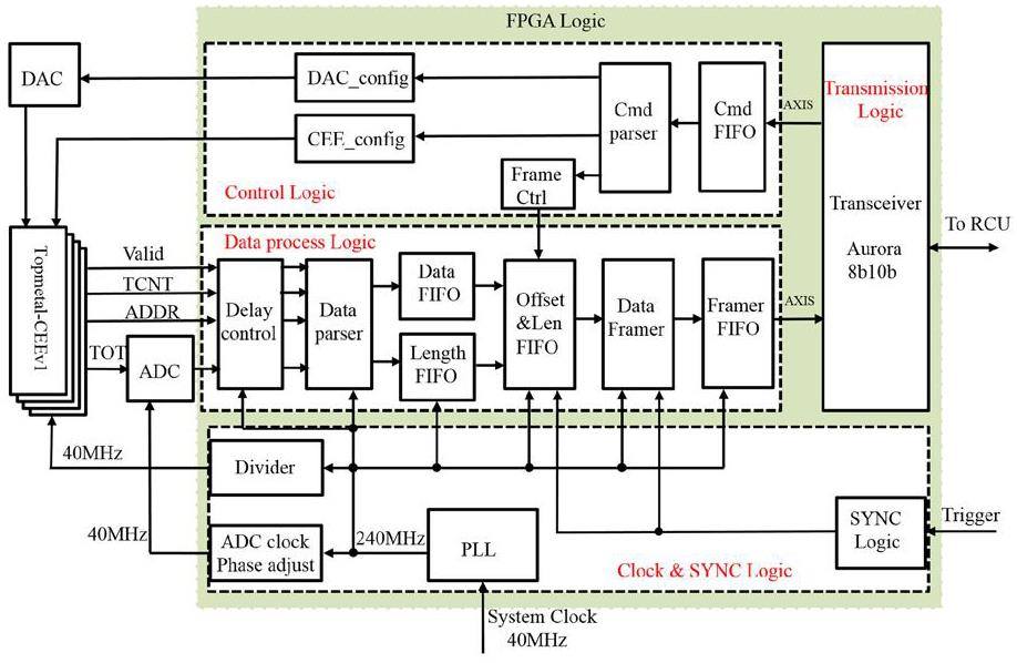
The data processing logic collects output data from Topmetal-CEEv1, including digital outputs (Valid, ADDR, and TCNT signals) and analog outputs (TOT signals). In Topmetal-CEEv1, the TOT pulse width is converted into an analog signal, which is then digitized using an off-chip 8-channel ADC. The sampling clock of the ADC is 40 MHz, which is the same frequency as that of Topmetal-CEEv1. Owing to the additional delay resulting from the ADC digitization, a delay control module is designed to adjust the relative delay between the digitized TOT signals and the digital outputs of the chip. After the data are aligned using the delay control logic, they are sent to the data parser module for processing. The Valid signal is used to determine whether the data are stored in the Data FIFO. Because of the data-driven nature of the chip, the data frame is defined with an interval time of a certain length, which is set to 1 μs for now. Only the valid data within this 1 μs are stored in the data frame. Moreover, the length of the data frame is stored in the Length FIFO. When the FEC receives the trigger signal, the data framer reads some consecutive frames from the FIFO and forms a larger frame according to the frame format required by the DAQ. To prevent FIFO overflow, the framed data with the earliest timestamp are discarded if the FIFO is approximately 96% full. The frame is then sent to the transmission FIFO of the high-speed serial transceiver. The protocol is Aurora 8B/10B [44], which is a Xilinx LogiCORE IP designed to enable the easy implementation of transceivers for high-speed serial communication. The command from the RCU can control the number of frames to be read and the offset time of these frames relative to the trigger time. Simultaneously, the control logic can configure the DAC to generate bias voltages and configure the registers in the Topmetal-CEEv1 chips. The functions of the synchronization module include timestamp synchronization, timestamp zeroing, and generation of data flow control signals and trigger signals. The system clock of the FEC is 40 MHz as provided by the SCM. The PLL [45] in the FPGA is used to generate a 240 MHz clock for the data framer, a 40 MHz clock for the Topmetal-CEEv1 chip, and a 100 MHz clock for the AXIS [46] bus.
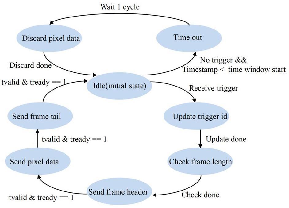
A state–machine diagram of the FEC is shown in Fig. 7. Upon receiving the trigger signal, it updates the trigger ID and sends the framed pixel data to the DAQ within a predefined time window. Whenever there is no trigger signal, pixel data with a timestamp earlier than the time window are discarded.
Readout and Control Unit design
Hardware
The RCU is a standard 6U CPCI card based on the Xilinx Kintex-7 FPGA XC7K325T. The CPCI crate is only used for power supply and mechanical support and not for data transmission. Figure 8 shows a block diagram and photograph of the RCU. The interface between the RCU and the DAQ is an optical link. The RCU receives the 40 MHz system clock and trigger signals from the SCM and STM. The corresponding interfaces are differential and single-ended LEMO connectors, respectively. After the signal fan-out, the clock and trigger signals are sent to the RCU and FECs. Two SAMTEC coaxial connectors are adopted to connect the two FECs. The LEDs on the front panel are used to display the working states of the board, including but not limited to the power, temperature, and FPGA configurations. A 256 Mb SPI flash is used to store firmware, which can be remotely updated. To cache the data, four DDR3 memory chips with a total capacity of 1 GB are added to the board. The clock module generates the local system clock and transceiver reference clock. A temperature and humidity sensor is also included to monitor the status of the board.
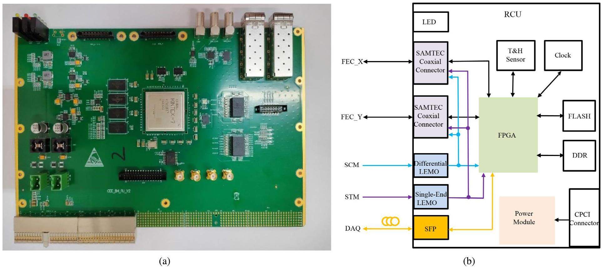
Two MPM54504 quad-output DC-DC modules and an LDO are used to generate the required voltages for the RCU. The current in each channel in the DC-DC module is 5 A. The ADCs are powered by the LDO owing to its low-noise feature. Two MP1495 DC-DC converters are used to power the front-end electronics. The currents in the RCU and the front-end electronics can both be monitored. Once the currents exceed the preset thresholds, the DC-DC converters can be shut down by disabling the control pin.
Firmware
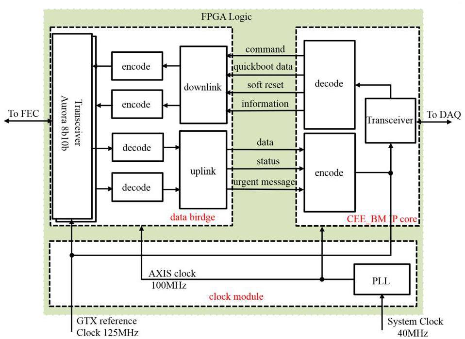
Figure 9 shows the block diagram of the RCU logic. The FPGA logic of the RCU is primarily divided into three main components: the clock module, DAQ interface, and FEC interface. The clock module manages the FPGA's internal clock system. Using a PLL, it converts the 40 MHz main clock into a 40 MHz AXIS bus clock and the other working clocks required by various modules. Simultaneously, this module transmits the 125 MHz clock from the PCB board to the interface sections as their reference clock. The DAQ interface module hosts an IP core named CEE_BM, which is primarily tasked with communicating with the DAQ, transmitting various signals including commands and data. Additionally, this module handles soft resets and provides quick boot functionality to the beam monitoring system. The FEC interface module acts as a bridge between the RCU and the two FEC units, consisting of uplink and downlink channels. The downlink channel encodes commands, whereas the uplink channel decodes data. Eventually, these data are transmitted to the FEC units using the Aurora 8b10b protocol.
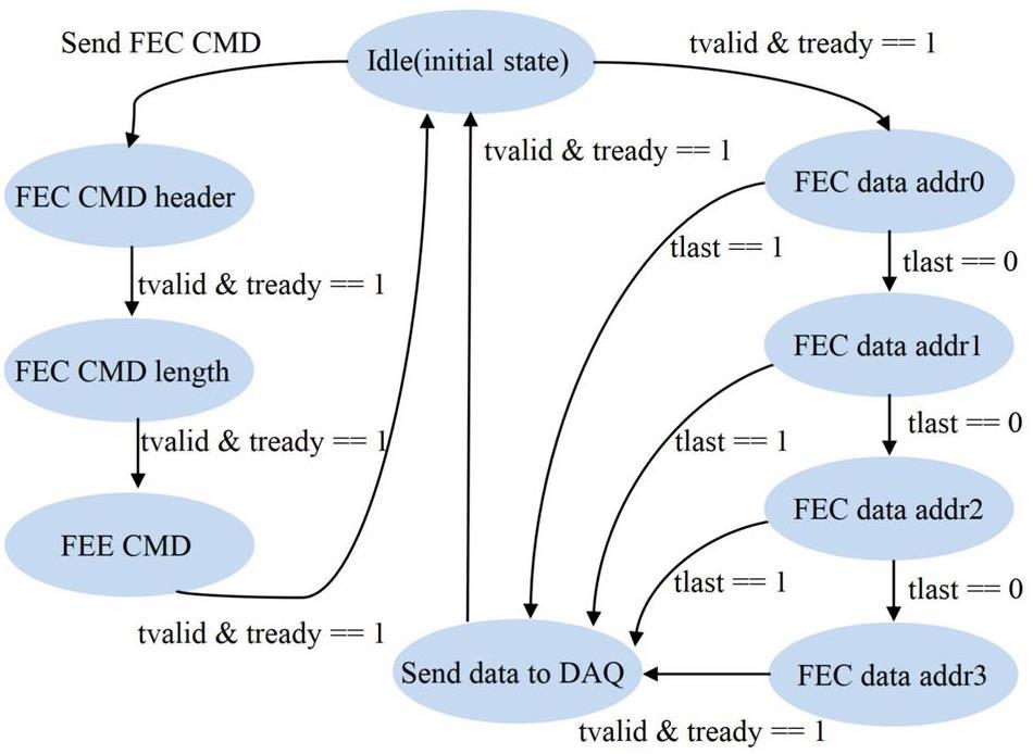
A state–machine diagram of the RCU is shown in Fig. 10. In one direction, it parses commands from the DAQ and sends them to the FECs; in the other direction, it receives data from the FECs and transfers them to the DAQ.
Experimental Results and Discussion
Tests have been performed to verify whether the designed functions of the electronics were fulfilled in order to evaluate the system's performance and check its responses to the particles of the radiation source and heavy-ion beam. More advanced characteristics, such as the dependence of its performance on the temperature and radiation level, as well as its data error rate in the targeted working environment, are still being studied and will be addressed in a separate publication.
Basic electronic functionality
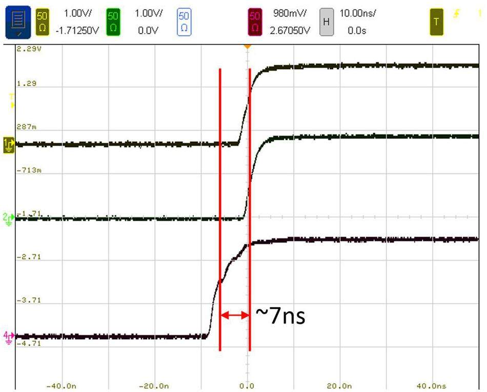
The main electronic test between the beam monitor and clock system is the global time synchronization test. Each subdetector has a 56-bit local global timestamp counter. The global time synchronization mechanism ensures that all subdetectors have consistent timestamp information. Owing to the different topological structures of the subdetectors, the timestamp counters are inconsistent after the system is powered on. The DAQ distributes a timestamp clear command to the MTM. After receiving the clear command, the MTM resets the local timestamp and sends a clear command with its timestamp information to the subdetectors. After receiving the clear command, the subdetector considers the path delay and parsing time to align the local timestamp with the MTM. To validate whether the global timestamp synchronization is successful, the bit of the MTM counter is compared to the corresponding bit of the subdetector local timestamp counter in an oscilloscope. If the signal skew is within a system clock cycle of 25 ns, synchronization is considered successful. Figure 11 shows that the signal skew is approximately 7 ns after timestamp synchronization.
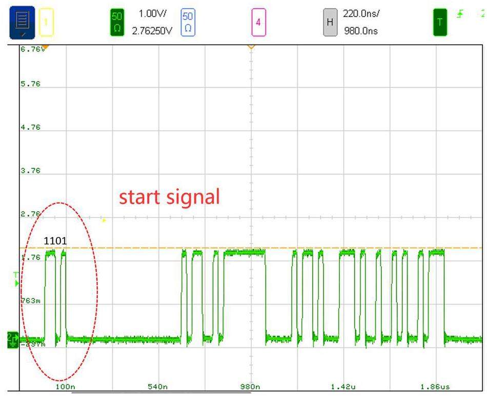
In addition to the trigger signal, the trigger system must distribute four other signals: the start, stop, clear, and sync signals. The effective pulse width of the trigger signal is one clock cycle of 25 ns. The other four signals are identified based on the effective pulse width of 2 clock cycles. The following 2 bits are used to indicate the command type. This is followed by 56 bits of timestamp information and 16 bits of trigger number information. A test with the trigger system showed that the electronics could successfully receive and parse the signals. Figure 12 shows the start signal observed using an oscilloscope.
The test between the beam monitor and DAQ mainly includes two parts: a command downlink and a data uplink. The DAQ configures the DAC to generate the correct voltages. Moreover, the Topmetal-CEEv1 chip can be configured through the SPI interface by the DAQ, enabling actions such as resetting the chip, changing the gain of the chip, and enabling and disabling the pixels. All designed communications with the DAQ have been tested and verified during the joint heavy-ion beam test described in Sect. 5.3.
The static power dissipation for one FEC is approximately 5 W, as described in Sect. 3.3.1.
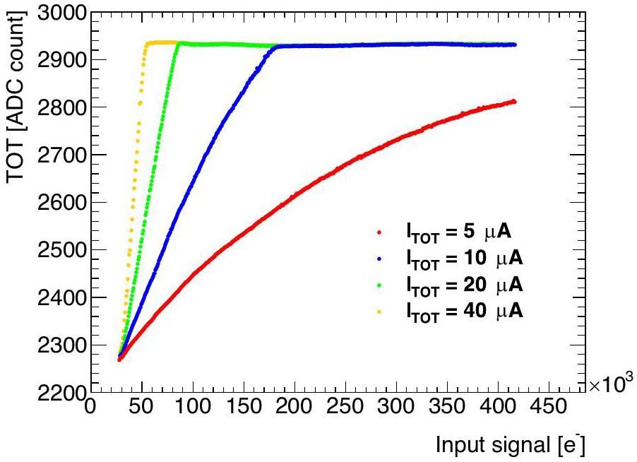
The input dynamic range of the electronics can be tuned by setting the charging current of the TOT in the Topmetal-CEEv1 chip. Figure 13 shows the measured amplitude as a function of the size of the input signal for the charging currents of 5 μA to 40 μA for one pixel. For a charging current of 5 μA, the input dynamic range exceeds 400 ke-. The distributions exhibit a logarithmic shape, particularly for a low charging current, where the input dynamic range is large. These distributions were obtained for each pixel to calibrate the amplitude measurement.
The temporal noise of the pixels is approximately 350 e- at a threshold of 30 ke- for a simplified readout system [27]. In the current readout electronics, this increases to approximately 720 e-. Several factors have been identified to explain this degradation, including the proximity of the FPGA and ADC to the chips and the clock distribution scheme of the chips. This problem will be mitigated in the updated version of the electronics. The resolution of the amplitude measurement using the TOT method is approximately 2.5 ke- for a 100 ke- signal. This large amplitude resolution is primarily due to the disturbance of the analog TOT signal caused by the digital circuit in the chip, which will be resolved in the updated version of the Topmetal-CEE chip.
The rate capability of the readout electronics system depends on several factors. First, the CSA of the pixels of the Topmetal-CEEv1 chip is designed to handle consecutive signals with a minimum time interval of approximately 0.5 μs. Owing to the high-gain setting of the CSA in the Topmetal-CEEv1 chip [27], the minimum time interval has been estimated to be approximately 1 μs using injected signals. Second, the maximum readout speed of the chip is 40 MPixels/s, which has also been verified using the injected signals. Given that one pixel is represented by 6-byte data, 40 MPixels/s translates to 1.92 Gbps. Third, the transfer speed between the FEE and RCU has been evaluated to be approximately 4 Gbps, which corresponds to 3.2 Gbps effective speed considering the 8b10b protocol. It is estimated that a single beam particle fires an average of approximately 10 pixels in one chip and 30 pixels in one FEC. Assuming a particle rate of 106 s-1, a readout speed of 10 MPixels/s is required for one chip, and a readout speed of 30 MPixels/s is required for one FEC. This corresponds to a 1.44 Gbps readout speed between the FEC and RCU, which can be achieved using the readout electronics.
The precision of time measurement is limited by the step size of the 8-bit counter of the chip, as described in Sec. 3.1, which is the same as the clock cycle at 25 ns. This has been verified using injected signals.
The measured results are summarized in Table 2.
| Temporal noise of the pixels | 720 e- |
| Resolution of amplitude measurement | 2.5 ke- |
| Input dynamic range | > 400 e- |
| Shaping time | ∼ 1 μs |
| Precision of time measurement | 25 ns |
| Maximum readout speed of chip | 40 MPixels/s |
| Maximum data transfer speed between FEE and RCU | 4 Gbps |
Performance with α particles
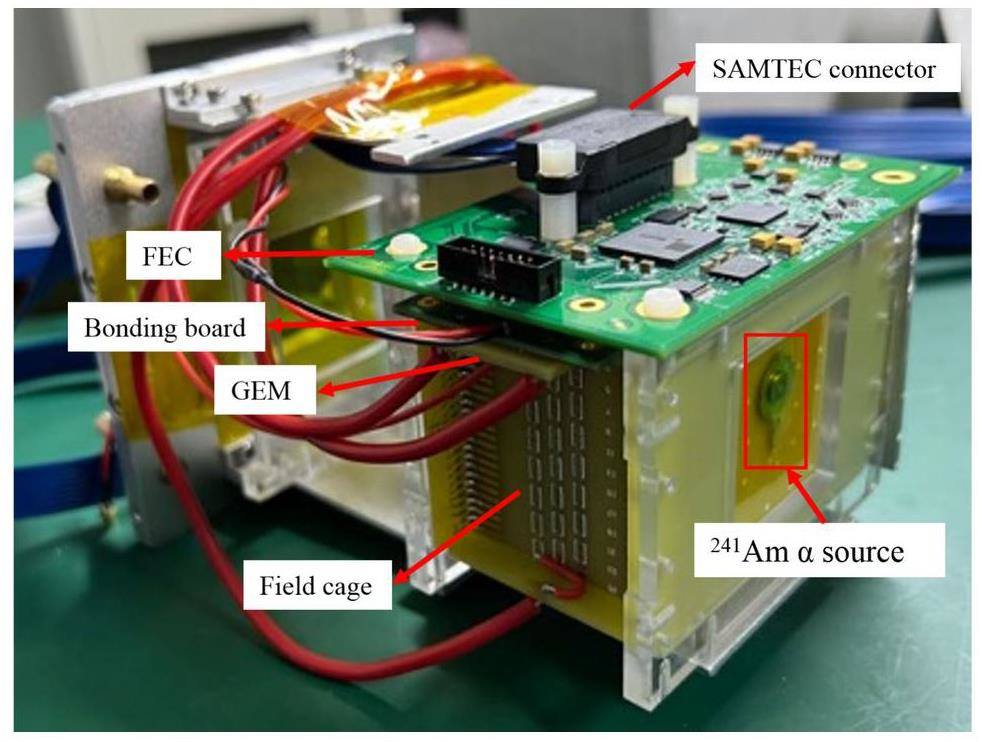
An 241Am α source is placed immediately outside the field cage, about the center in the plane transverse to the beam direction, in which the α particles enter the sensitive region through a hole in the Kapton film of the cage. A photograph of the setup is shown in Fig. 14. Its purpose is to monitor the status of the detector system by checking its response to the α particles under several benchmark detector configurations. Specifically, it reveals whether the high-voltage system, gas system, and electronic system are working as expected. Because the effective rate of the source is less than 100 Hz, it has an almost negligible impact on the test with heavy-ion beams, for which the rates are at least two orders of magnitude higher.
Using the α source, the hit maps of the chips over a duration of approximately 2.5 hours are shown in Fig. 15. This was measured in a gas mixture of Ar(70%)+CO2(30%) with a drift electric field of 300 V/cm, an induction electric field of 1000 V/cm, a VGEM of 400 V, and pixel charge thresholds of approximately 33 ke-. This high pixel charge threshold is intended to prevent the unusually large spike noise due to the disturbance caused to the analog circuit by the digital circuit, as found in Ref. [27]. Figure 15a shows the inclusive hit map, whereas Fig. 15b-d, and 12 show the hit maps with the requirements of the α tracks of hits in exactly one, two, and three rows of the pixels, respectively. The blank areas indicate areas not covered by the CCEs of the chips. The center of the chip in Row-0 is approximately the closest to the α source.
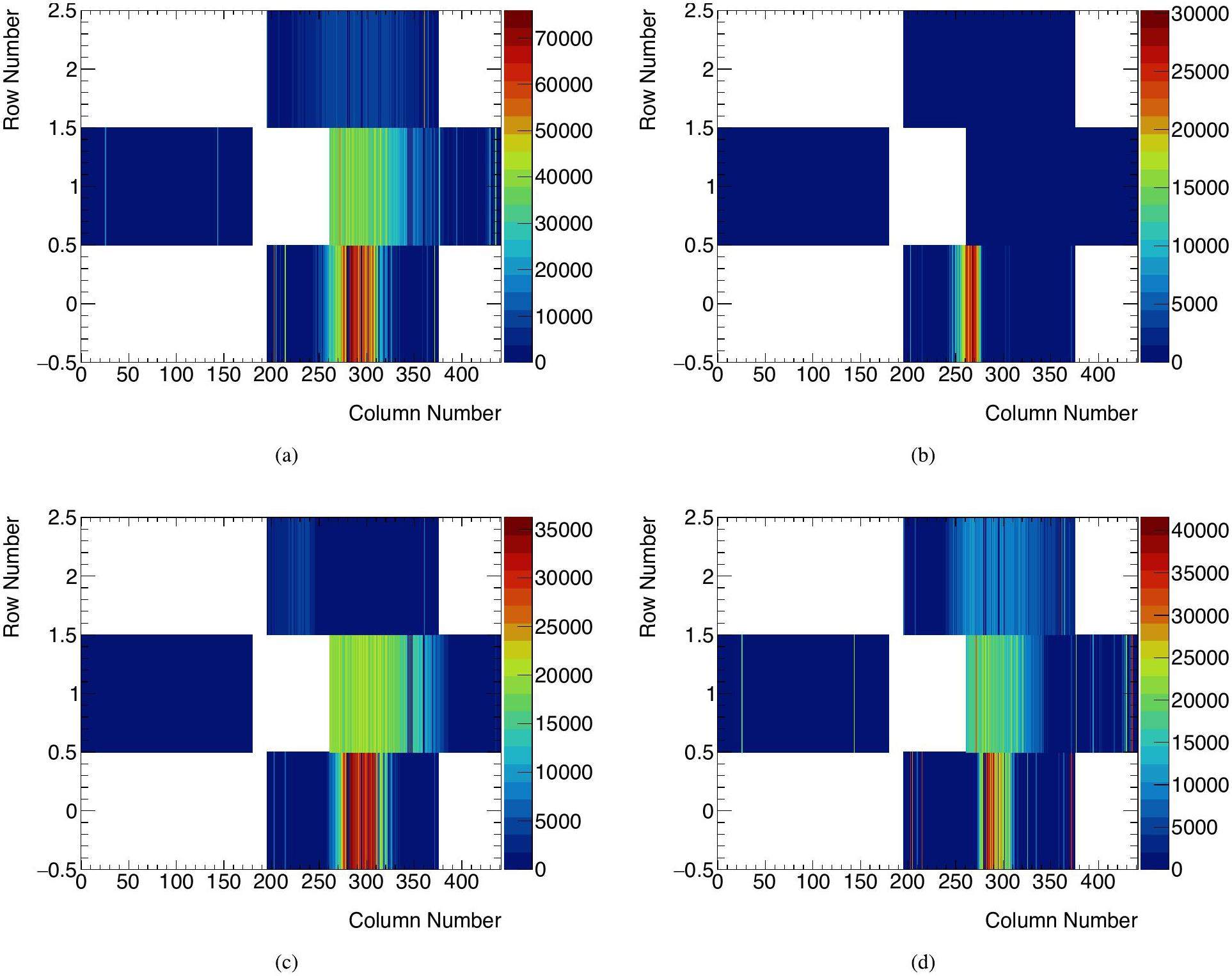
Owing to the large dispersion of the pixel thresholds, as described in Ref. [27], the number of hits does not exhibit a smooth distribution across the pixels. Several instances of noise or dead pixels can also be seen in the plots. Both methods require careful treatment and rigorous analysis.
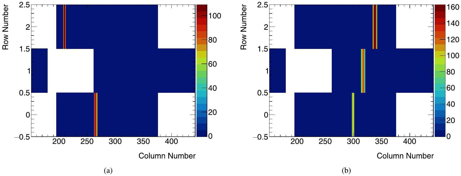
Two typical α tracks of hits in two and three rows of pixels are shown in Fig. 16a, b, respectively. The color of the plots corresponds to the amount of charge in units of about 700 e-. The pixels in the center of the pixel cluster yield larger signals, subject to fluctuations in the the gains of the GEM, ionization processes, and pixel responses. Using these settings for the pixel charge threshold and VGEM, the average number of hits in each row of pixels is approximately five.
Joint heavy-ion beam test with other CEE subsystems
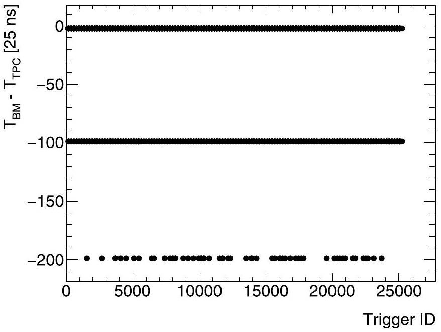
The beam monitoring system, together with all the other subsystems of the CEE spectrometer except for the magnet, underwent a one-week-long joint test using the heavy-ion beam facility at HIFRL-CSR. The test was conducted in the newly decorated hall to host the eventual CEE spectrometer, and all CEE subdetectors, although not necessarily in their full-sized versions, were placed approximately according to the designed geometry, as shown in Fig. 1. The type of ion was Kr of approximately 320 MeV/u with an intensity varying between approximately 104 pps and 106 pps. Regarding the beam monitor, the primary purpose of the test was to verify the functionalities of the electronic system, particularly in terms of its communication with the DAQ, trigger, and clock systems, as well as its stability. The electronic system operated smoothly during the test. Figure 17 shows the difference between the timestamps provided by the beam monitor and the TPC as a function of the trigger ID. The value was set to -199 (-99) in the case of no valid beam monitor (TPC) data corresponding to the trigger ID. Although the beam monitor was expected to provide valid data for every fired trigger, there was a defect in the readout firmware, resulting in dead time during the data transfer. Because clock synchronization was not accurately performed for the subdetectors before the test, the plot shows a stable constant value of -5 clock cycles (25 ns) across all trigger IDs.
Another goal was to determine whether the electronics could withstand radiation in an environment similar to that of the designed experiment. No single-event effect was observed in the one-week test.
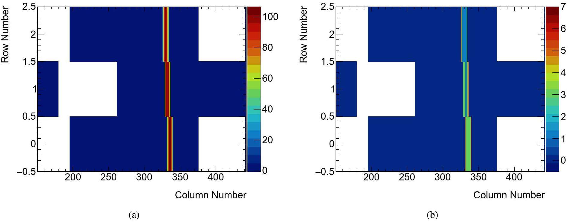
The two plots in Fig. 18 show a typical ion track, where the color of the plots represents the signal amplitudes (18a) in units of approximately 700 e-, and time (18b) in units of 25 ns. The signal time is represented by a 56-bit unsigned integer in the DAQ system. For illustration, in Fig. 18b, the color indicates the relative signal time, with the earliest set to 1. It was measured using the same detector configurations as those used for the α tracks, except for the VGEM of 350 V and pixel charge thresholds of approximately 22 ke-. It can be seen that the pixels in the center of the pixel cluster yielded larger signals and earlier timestamps, which is consistent with expectations. As mentioned in Ref. [27], in the Topmetal-CEEv1 chip, the digital circuit causes a large disturbance to the analog circuit, which forces a minimum threshold of about 20 ke-. Consequently, during the beam test, the GEM had to be operated in large-gain configurations that could not withstand the intensity of the beam. To mitigate this issue, an updated version of the Topmetal-CEE chip has been designed.
Conclusion
The readout electronics for the beam monitor have been designed and the corresponding boards have been produced and assembled. The system includes two bonding boards carrying the Topmetal-CEEv1 chips, two FECs, and one RCU. Charges from the ionization process are captured by the CCEs of the Topmetal-CEEv1 chips, and are transmitted to the FECs after amplification and discrimination in the chip. After framing and packaging in the FECs, the data are transmitted to the RCU, which communicates with the DAQ, trigger, and clock systems. The firmware of the FECs and RCU performs command parsing, data processing, and transmission. All designed functionalities of the system were verified through electronic tests, and the system's responses to α particles and heavy-ion beams were also investigated. The results prove that this readout electronics system satisfies the basic requirements of the beam monitor. To further improve the detector performance, an updated Topmetal-CEE chip has been developed. More work will be done to accommodate the system in different running modes of the CEE experiment, the specifications of which are yet to be finalized.
The heavy ion cooler-storage-ring project (HIRFL-CSR) at Lanzhou
. Nucl. Instrum. Meth. A 488, 11 (2002). https://doi.org/10.1016/S0168-9002(02)00475-8Nuclear matter at a HIRFL- CSR energy regime
. Nucl. Part. Phys. 36,Status of the HIRFL-CSR complex
. Nucl. Instrum. Meth. B 317, 214 (2013). https://doi.org/10.1016/j.nimb.2013.07.040Conceptual design of the HIRFL-CSR external-target experiment
. Sci. China Phys. Mech. Astron. 60,A study of the properties of the QCD phase diagram in high-energy nuclear collisions
. Particles. 3, 278-307 (2020). https://doi.org/10.3390/sym15020499Design and tests of the prototype beam monitor of the CSR external target experiment
. Nucl. Sci. Tech. 33, 36 (2022). https://doi.org/10.1007/s41365-022-01021-1The Topmetal-CEE prototype, a direct charge sensor for the beam monitor of the CSR externaltarget experiment
. J. Instrum. 17,Readout Electronics of the Prototype Beam Monitor in the HIRFL-CSR External-Target Experiment
. Electronics. 11, 2679 (2022). https://doi.org/10.3390/electronics11172679A Gaseous Beam Monitor for the CSR External-Target Experiment
. Phys. Atom. Nuclei. 86, 1411-1415 (2023). https://doi.org/10.1134/S1063778823060212Simulation Studies of the Beam Monitor for the CSR External-Target Experiment
. Phys. Atom. Nuclei. 86, 1416-1420 (2023). https://doi.org/10.1134/S1063778823060224Beam test study of the MRPC based T0 detector for the CEE
. J. Instrum. 14,Readout Electronics of T0 Detector in the External Target Experiment of CSR in HIRFL
. IEEE Trans. Nucl. Sci. 65, 1315-1323 (2018). https://doi.org/10.1109/TNS.2021.3093544Laser test of the prototype of CEE time projection chamber
. Nucl. Sci. Tech. 29, 41 (2018). https://doi.org/10.1007/s41365-018-0382-4Simulation of momentum resolution of the CEE-TPC in HIRFL
. Nucl. Sci. Tech. 39, 70401 (2016). https://doi.org/10.1007/s41365-018-0382-4Advances in nuclear detection and readout techniques
. Nucl. Sci. Tech. 34, 205 (2023). https://doi.org/10.1007/s41365-023-01359-0Development of multichannel readout electronics prototype system for TPC detector of CSR External-Target Experiment
. Nucl. Instrum. Meth. A 1052,Readout Electronics Prototype of TOF Detectors in CEE of HIRFL
. IEEE Trans. Nucl. Sci. 68, 8 (2021). https://doi.org/10.1109/TNS.2021.3093544CEE inner TOF prototype design and preliminary test results
. J. Instrum. 17,Simulation and prototype testing of multi-wire drift chamber arrays for the CEE
. Nucl. Sci. Tech. 31, 11 (2020). https://doi.org/10.1007/s41365-019-0716-xA tracking system for the external target facility of CSR
. Nucl. Sci. Tech. 28, 68 (2017). https://doi.org/10.1007/s41365-019-0716-xDevelopment of a multi-channel readout electronics verification system for MWDC detectors
. Radiat. Detect. Technol. Methods 6, 281-288 (2022). https://doi.org/10.1007/s41605-022-00347-zBeam test result of the sealed MRPC prototype for CEE-eTOF
. J. Instrum. 18,The CEE-eTOF wall constructed with new sealed MRPC
. J. Instrum. 15,Classifier for centrality determination with zero-degree calorimeter at the cooling-storage-ring external-target experiment
. Nucl. Sci. Tech. 34, 176 (2023). https://doi.org/10.1007/s41365-023-01338-5Event plane determination from the zero degree calorimeter at the cooling storage ring external-target experiment
. Nucl. Sci. Tech. 34, 100 (2023). https://doi.org/10.1007/s41365-023-01262-8Readout Electronics for the Zero Degree Calorimeter at HIRFL-CEE Experiment
. IEEE Trans. Nucl. Sci. 70, 6 (2023). https://doi.org/10.1109/TNS.2022.3216453Design and preliminary characterization of a novel silicon charge sensor for the gaseous beam monitor at the CSR external-target experiment
. Nucl. Instrum. Meth. A 1047,A real-time online data acquisition system for Dragon-I linear induction accelerator
. Nucl. Sci. Tech. 28, 37 (2017). https://doi.org/10.1007/s41365-017-0182-2Design of a NIM-based DAQ system
. Nucl. Sci. Tech. 28, 139 (2017). https://doi.org/10.1007/s41365-017-0296-6Design of Data Acquisition System for TOF Detectors in the CEE Experiment
. Nucl. Phys. Rev. 38(3), 301-310 (2021). https://doi.org/10.11804/NuclPhysRev.38.2020070Event Building Algorithm in a Distributed Stream Processing Data Acquisition Platform: D-Matrix, IEEE Trans
. Nucl. Sci. 70, 2 (2023). https://doi.org/10.1109/TNS.2023.3235904Preliminary design of a femtosecond timing system for large accelerator facilities
. Nucl. Sci. Tech. 29, 32 (2018). https://doi.org/10.1007/s41365-018-0369-1The Clock System in Readout Electronics System for the External Target Experiment in CSR of HIRFL
. J. Instrum. 14,An FPGA-based trigger system for CSHINE
. Nucl. Sci. Tech. 33, 162 (2022). https://doi.org/10.1007/s41365-022-01149-0The trigger system for the CSR external-target experiment
. (2023). https://doi.org/10.48550/arXiv.2307.07692A 12-bit 1.25 GS/s RF sampling pipelined ADC using a bandwidth-expanded residue amplifier with bias-free gain-boost technique
. Microelectronics Journal 130,A 1-GS/s, 12-b, Single-Channel Pipelined ADC With Dead-Zone-Degenerated Ring Amplifiers
. Journal of Solid-State Circuits 54, 646-658 (2019). https://doi.org/10.1109/JSSC.2018.2889680Multiple time-over-threshold readout electronics for fast timing and energy resolving in a SiPM-based positron annihilation lifetime spectrometer
. J. Instrum. 15,The TaichuPix1: a monolithic active pixel sensor with fast in-pixel readout electronics for the CEPC vertex detector
. J. Instrum. 16,Low-power priority address-encoder and reset-decoder data-driven readout for monolithic active pixel sensors for tracker system
. Nucl. Instrum. Meth. A 785, 61 (2015). https://doi.org/10.1016/j.nima.2015.02.063A low-noise CMOS pixel direct charge sensor, Topmetal-II
. Nucl. Instrum. Meth. A 810, 144 (2016). https://doi.org/10.1016/j.nima.2015.11.153Topmetal-II-: A direct charge sensor for high energy physics and imaging applications
. J. Instrum. 11,Topmetal-M: A novel pixel sensor for compact tracking applications
. Nucl. Instrum. Meth. A 981,Aurora 8B/10B LogiCORE IP Product Guide
.Design and Emulation of All-Digital Phase-Locked Loop on FPGA
. Electronics 8, 11 (2019). https://doi.org/10.3390/electronics8111307AXI Reference Guide
.The authors declare that they have no competing interests.


