Introduction
Since their discovery, X-rays have been extensively used in diagnostic imaging [1], radiotherapy [2], public safety [3], and material engineering [4]. Currently, X-rays are mostly generated by thermoelectric X-ray tubes, in which electrons are emitted by heating a filament and then accelerated to bombard the anode target. However, these thermoelectric tubes suffer owing to their bulkiness, high-energy consumption, and cumbersome thermal management systems [5, 6]. Following the advancement of microfabrication techniques, cold-cathode X-ray sources have gained attention owing to their advantages of compactness, low-energy consumption, and fast response [7-9]. For example, carbon nanotube X-ray sources have been successfully fabricated and commercialized [10, 11], offering advantages in stationary X-ray imaging [12, 13]. However, these are still single-focus X-ray sources, and are limited by the long source-to-patient distance.
In contrast, a novel cold cathode, flat-panel, X-ray source (FPXS) consisting of multiple X-ray emitting units integrated on a single substrate has been proposed [5]. Based on the advantages of ZnO nanowires, such as easy large-area fabrication and uniform electron emission [14], our team fabricated a ZnO nanowire FPXS and achieved high-contrast X-ray imaging [15]. With the development of microfabrication technology, a more flexible two-dimensional addressable ZnO nanowire FPXS has been developed by preparing ZnO nanowire strips on a cathode panel and molybdenum (Mo) film strips on an anode panel [16]. The intersection of the cathode and anode forms multiple addressable X-ray-emitting units. The addressable ZnO nanowire FPXS has several key advantages. First, it selectively emits photons on demand, reducing the radiation dose to the imaged samples [15]. Second, it can reduce motion artifacts related to gantry rotation by replacing mechanical motion with periodic photon emissions from array sources [17]. Furthermore, the dynamic range of electron bombardment in the anode prevents heat accumulation in a single area and reduces anode loss [18]. Given the advantages of addressability and distributed X-ray sources [19], the ZnO nanowire FPXS may provide novel X-ray applications such as stationary computed tomography [17] and grating-based phase-contrast imaging [20].
The performance of the X-ray source can be improved by optimizing the material, thickness, and morphology of the anode [21-23]. Experimental analysis of the X-ray characteristics and optimizing the anode of the X-ray source are time-consuming and expensive. MC simulation is an accurate, efficient, and cost-effective method for simulating particle transport [24, 25]. The methodology used to optimize and analyze thermoelectric X-ray sources using MC simulations is well established [26-28]. As the benefits of FPXS have become apparent, MC simulation studies of FPXS have been conducted. For example, G rant et al. optimized the anode target, analyzed the X-ray energy spectrum and angular distribution of a carbon nanotube FPXS [29]. In a subsequent study, they examined the impact of a collimator on an FPXS based on nitrogen-incorporated ultrananocrystalline diamond [30]. However, these findings were limited to FPXS, which has a small emission area. In one of our previous research study, we obtained the optimal thickness of a thin tungsten (W) target at 40 kV for ZnO nanowire FPXS [31]. Nevertheless, the emission characteristics of ZnO nanowire FPXS have not been fully explored, and the parameters under consideration for optimization are incomplete.
In this study, we addressed the gaps described above by optimizing the ZnO nanowire FPXS in terms of both the anode and substrate of the anode panel. The key X-ray characteristics, including the average fluence, average energy, and spatial distribution, were also analyzed using MC simulations. The accuracy of the MC simulations was verified by comparing the measured energy spectra with the simulated energy spectra. Regarding the anode morphology, we considered two microstructural morphologies, namely those of a microstriped array and a microsemiellipsoidal anode. The optimal thicknesses of the W and Mo microstriped array anodes were obtained with acceleration voltages in the range of 30–90 kV, and the X-ray spatial distribution of the microstriped array anode was analyzed. We studied the variation trend of the X-ray fluence with the raised and recessed degrees of the microsemiellipsoidal anode and explored the underlying reasons for this trend through energy conversion experiments of the incident electrons. To optimize the substrate, the X-ray filtering effect and physical properties of different thicknesses of different materials were considered. The findings of this study can provide valuable guidance for the fabrication of the ZnO nanowires FPXS, ultimately reducing the number of development cycles and cost. The optimized ZnO nanowire FPXS obtained in this study can be used in a novel medical imaging modality.
Materials and methods
ZnO nanowire cold cathode FPXS
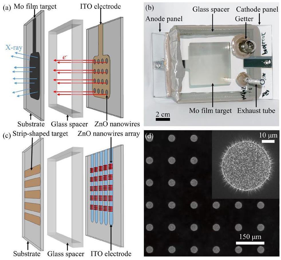
Several ZnO nanowire FPXSs were successfully fabricated. Herein, we introduce two representative FPXSs: a film-target ZnO nanowire FPXS [32] (Fig. 1(a)), and an addressable ZnO nanowire FPXS [16] (Fig. 1(c)). A schematic of the film-target ZnO nanowire FPXS is shown in Fig. 1(a). The FPXS is composed of a transmission-type anode panel and field-emission cathode panel. The anode panel had a Mo-film target deposited on a glass substrate. The cathode panel was fabricated by depositing patterned Zn arrays on a glass substrate coated with indium tin oxide (ITO). The patterned Zn arrays were then converted into ZnO nanowire field emitter arrays via thermal oxidation. A glass spacer was used to maintain a fixed distance between the anode and cathode panels. When a sufficiently high voltage was applied, a field-emission effect occurred, and electrons were emitted from the ZnO nanowires. These electrons were then accelerated and bombarded on the anode to produce X-rays. Figure 1(b) shows a photograph of an encapsulated ZnO nanowire FPXS with a Mo-film target. An exhaust tube and getter were installed on the cathode panel for vacuum pumping. Figure 1(c) shows a schematic of an addressable ZnO nanowire FPXS. The anode panel was composed of five strip-shaped Mo targets sandwiched between two thin aluminum (Al) films to prevent oxidation during the vacuum sealing process. The cathode panel consisted of five strip-shaped ITO electrodes arranged orthogonally to the anode. Addressable emission of X-rays can be achieved by selectively applying a high voltage between the anode strips and cathode electrodes. At the intersection of the cathode and anode strips, an array spanning 5 × 5 luminous pixels was obtained, resulting in 25 independent luminous pixels and a size 4.325 mm × 4.325 mm. Figure 1(d) shows the morphology of the ZnO nanowires field-emitter array characterized by scanning electron microscopy.
MC simulations of the ZnO nanowire FPXS
Geant4 is an accurate, reliable, flexible, and extensively accepted MC simulation software program [33]. In this study, Geant4 (version 11.02, CERN) was used to simulate the process of high-energy electrons bombarding the anode panel and the X-ray generation. Owing to the strong electric field between the cathode and anode, the direction of movement of the electrons produced by the ZnO nanowires was almost perpendicular to the anode panel; thus, a parallel electron beam was used to model the cathode. The number of simulated electrons was 5 × 10⁹. The range cutoff in Geant4, which represents the distance threshold for secondary radiation production, was set to 1 nm. The Penelope model was adopted because of its accuracy in the low-energy range [34].
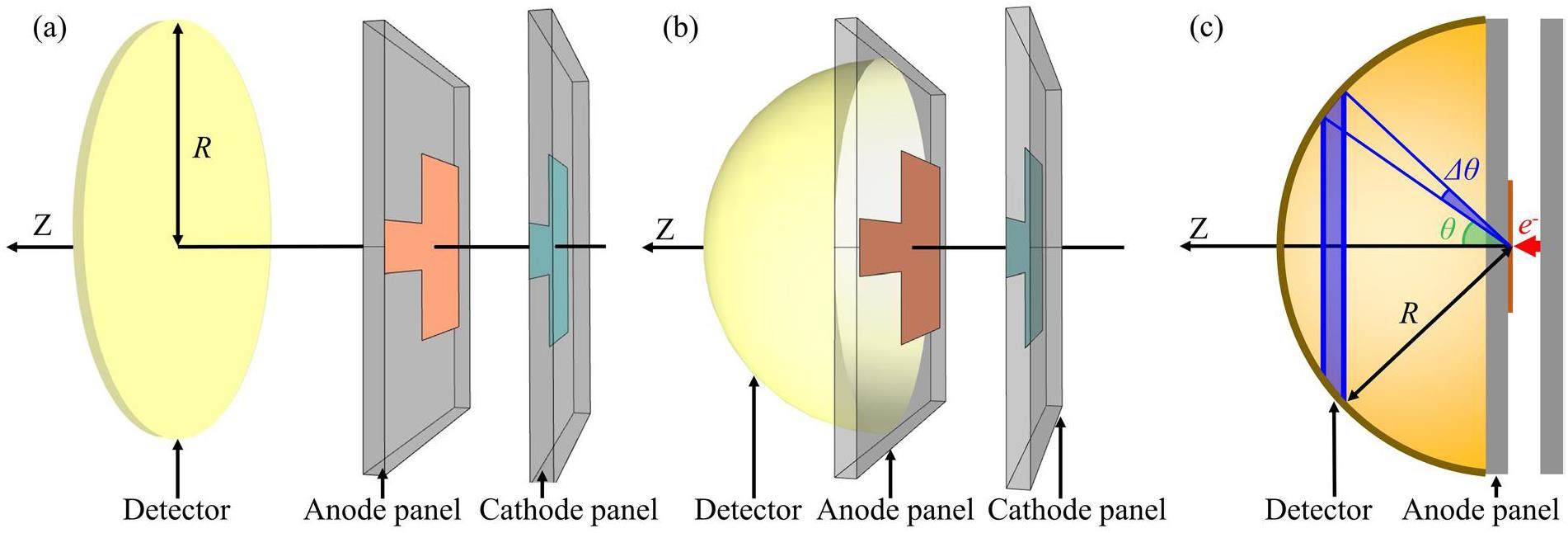
In the simulations, two X-ray detection modes were established to analyze the X-ray characteristics under different conditions. Specifically, the first mode was a planar detection mode used to detect the transmitted X-rays emitted from a large-area target, wherein a circular detector with radius R was placed parallel to the substrate, as illustrated in Fig. 2(a). The average fluence of the X-rays can be calculated by dividing the number of photons by the detector area. The average X-ray energy was determined by dividing the total photon energy by the number of photons. The second detection mode, referred to as hemispherical detection mode, was employed to investigate the divergence characteristics of the transmitted X-rays. In this mode, the hemispherical detector was placed at the center of the anode, as shown in Fig. 2(b)). On a hemispherical detector with radius R, Δθ around the emission angle θ corresponds to a spherical ring, as shown in the blue region in Fig. 2(c)). Δθ is a fixed angle bin used to divide the hemispherical detector into segments. When a specific θ was selected, the corresponding spherical ring was defined. The average fluence and energy of the X-rays at the emission angle θ were calculated based on the photons that reached the spherical ring. None of the detectors in the simulation affected the photon transport.
Experiments and evaluations
In this subsection, the accuracy of the MC simulations on the ZnO nanowire FPXS was first verified by comparing the measured and simulated energy spectra. The anode and substrate were then optimized using MC simulations. The average fluence and X-ray spatial characteristics of the microstriped array anode and the microsemi-ellipsoidal anode were investigated. Regarding the substrate, we analyzed the filtering effect of three types of substrate materials and the corresponding substrate thickness on X-rays.
Comparison between measured and simulated X-ray spectra
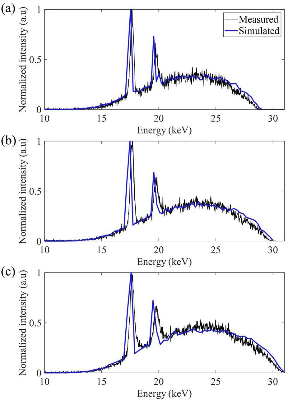
The ZnO nanowire FPXS shown in Fig. 1(c) were used as subjects for the comparative experiment. The measured spectra were recorded using an X-123 CdTe X-ray spectrometer (AMPTEK, Bedford, MA, USA). In the simulations, the thicknesses of Mo and Al were respectively set to 400 μm and 100 μm according to the actual FPXS. The electrons were sampled uniformly in an area of 5 × 5 luminous pixels. The acceleration voltages were set at 29, 30, and 31 kV, respectively. The simulated energy spectra were acquired in the planar detection mode with the detector located 10 cm away from the rear side of the anode’s substrate. To detect an adequate number of photons the detector’s R value was set to 5 cm. Air was filled in the area between the FPXS and detector to maintain consistency with the experimental setups.
Microstriped array anode thickness optimization and X-ray distribution
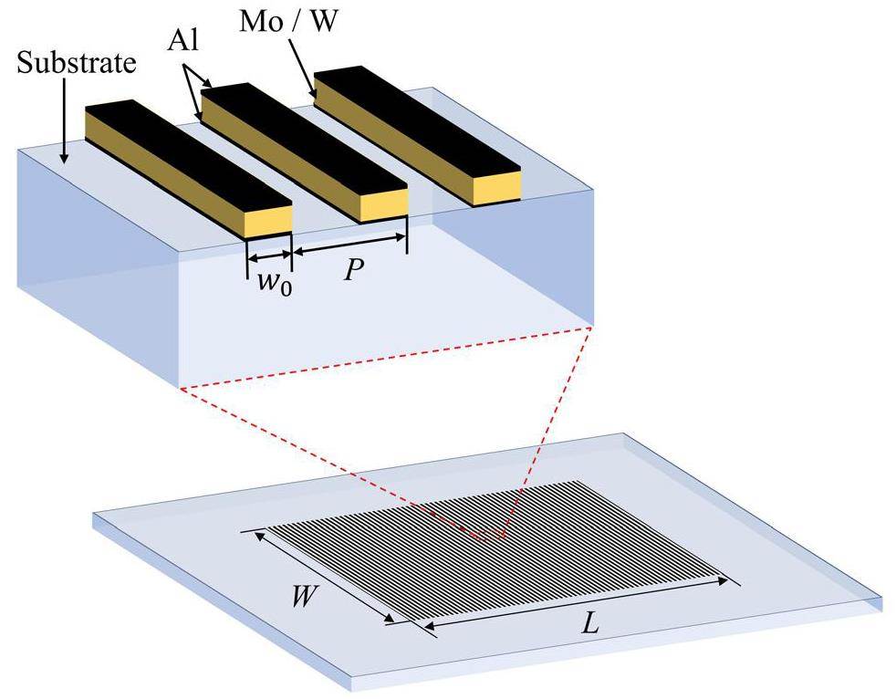
The microstriped anode array shown in Fig. 3 shows the base pattern for the anode of the addressable ZnO nanowire FPXS. The anode strips were arranged periodically on a glass substrate with a period (P) of 15 μm. The duty cycle (DC) was defined as
To optimize the thickness of the microstriped array anode for increased transmitted X-ray fluences, the average fluence for different thicknesses at the acceleration voltages of 30, 60, and 90 kV was obtained using MC simulations. The electrons were uniformly sampled over a 300 μm × 300 μm area in the center of the microstriped array anode because the anode was periodically distributed, thus reducing the simulation time. The simulations adopted a planar detection mode with R = 5 cm, and the distance from the detector to the rear side of the substrate was set to 5 cm.
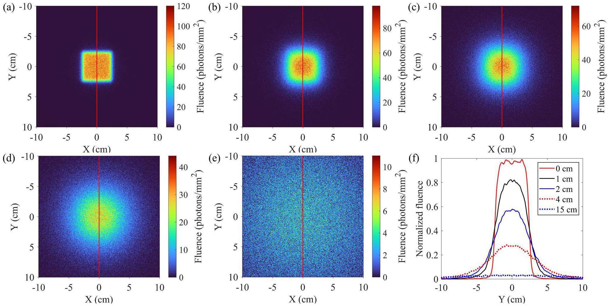
The investigation of the spatial distribution of the transmitted X-rays included the local distribution under the microstriped array anode and the overall distribution at different distances from the rear side of the anode substrate. A microstriped array Mo anode with P of 15 μm, 30 μm, and 60 μm was simulated at 60 kV. The electron bombardment area was set to 300 μm × 300 μm and 4.8 cm × 4.8 cm in the cases of the local and overall spatial X-ray distributions, respectively. A circular detector with R = 10 cm was placed under the microstriped array anode to obtain the local X-ray distribution, and five additional circular detectors were placed 0, 1, 2, 4, and 15 cm behind the rear side of the substrate to obtain the overall X-ray spatial distribution.
Effects of microsemi-ellipsoidal anode on X-ray generation
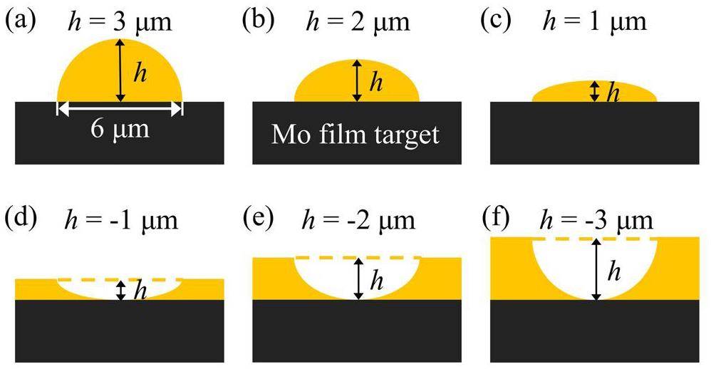
In this study, we investigated the transmitted X-ray characteristics of a microsemi-ellipsoidal structure on a film target, as shown in Fig. 4. The microsemi-ellipsoidal structure included raised and recessed designs. Raised-design microsemi-ellipsoidal structures were formed using a flattened semi-ellipsoid anode, as depicted in Fig. 4(a)-(c). Conversely, recessed microsemi-ellipsoidal structures were created by punching a semi-ellipsoidal hole on the thickened film target, while the thickness at the thinnest point was still set to 3 μm, as depicted in Fig. 4(d)-(f). The equatorial diameter of the microsemi-ellipsoidal structures was fixed at 6 μm, where h is the distance from the center to the pole along the symmetry axis. The values of h were set to values from -3 μm to 3 μm with a step size of 1 μm. Positive values of h correspond to the raised design and negative values correspond to the recessed design, with h = 0 μm for the film target. The thickness of the Mo film target was set to 3 μm, which is the optimal thickness for a fluence of 50 kV [36]. The electron source was configured as a pencil beam with a diameter of 6 μm to cover the microsemi-ellipsoidal structure. The acceleration voltage was set to 50 kV. The simulations were conducted in the hemispherical detection mode with R = 5 cm and Δθ was set to 5°. The reasons for the differences in the production of X-rays in different microsemi-ellipsoidal structures were also investigated. The energies of electron deposition at the anode, backscattered electrons, and photons generated within the anode were recorded in this study.
Effects of substrate material and thickness on X-ray filtering
The material and thickness of the substrate affect considerably the X-ray fluence because X-rays must pass through the substrate. Currently, the ZnO nanowire FPXS uses silica glass (SiO2) as the substrate material. In addition to silica glass, two additional substrate materials, namely synthetic sapphire (α-Al2O3) and silicon carbide (SiC) ceramics, were selected as candidate materials for the ZnO nanowire FPXS.
To evaluate the filtering effect of the three substrate materials on the X-rays, simulations were conducted using an addressable ZnO nanowire FPXS, as shown in Fig. 1(c). The anode of the addressable ZnO nanowire FPXS remained unchanged, whereas the substrate materials were SiO2, Al2O3, and SiC, with respective densities of 2.32 g/cm3, 3.97 g/cm3, and 3.16 g/cm3. For each substrate material, thicknesses ranging from 0.5 mm to 4 mm were considered. The electrons were sampled uniformly in an area of 5 × 5 luminous pixels. The simulations adopted a planar detection mode, and the distance from the circular detector (R = 5 cm) to the rear side of the anode substrate was set to 10 cm. A full vacuum environment was set up, and the acceleration voltage was fixed at 30 kV.
Results
Comparison between measured and simulated X-ray spectra
Figure 5(a)–(c) presents a comparison of the measured and simulated spectra at 29, 30, and 31 kV, respectively. The energy spectra were normalized using their respective maximum values to enable a direct comparison. The comparison shows a strong agreement between the measured and simulated energy spectra and the difference in the position of the K-shell peaks was within 0.26 keV, indicating the accuracy of the MC simulation for the ZnO nanowire FPXS. Furthermore, photons below 12 keV were eliminated after transmission through a 3 mm glass substrate.
Microstriped array anode thickness optimization and X-ray distribution
Figure 6(a)–(c) illustrate the average X-ray fluence of the W and Mo microstriped array anodes at 30, 60, and 90 kV at different anode target thicknesses. B-spline interpolation was used to interpolate the data between the calculated points on the curves. A similar trend in the average fluence was observed for both the materials as the target thickness increased. First, the average fluence increased considerably at increased target thicknesses. Subsequently, the maximum average fluence was achieved at a specific thickness, after which the average fluence gradually decreased at increasing target thicknesses. The optimal thicknesses of the W and Mo targets based on the average fluence at all the tested acceleration voltages are shown in Fig. 6(d). The optimal thicknesses of the W target at the three acceleration voltages are 0.65 μm, 2.45 μm, and 5 μm, while the Mo target has optimal thicknesses of 1.45 μm, 5.25 μm, and 24 μm, respectively.
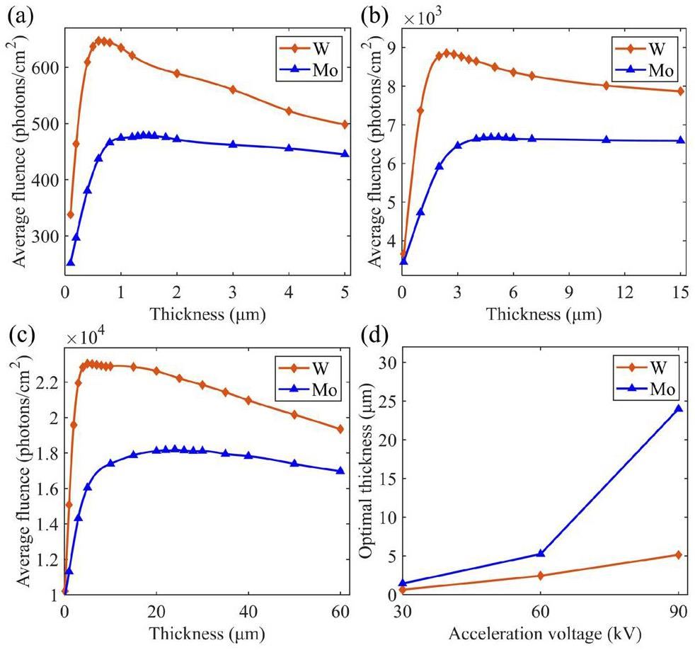
Figure 7(a)-(c) presents the local X-ray spatial distribution under the microstriped array anode with the P value set to 15 μm, 30 μm, and 60 μm, respectively. The results reveal a periodically patterned X-ray spatial distribution, where regions with high fluence correspond to the positions of the anode strips. Fig. 7(d) shows the normalized fluence profile along the red line in Fig. 7(a)-(c). The profile shows that although the X-rays were periodically distributed along the repetition direction of the anode stirps, the distribution did not exhibit a rectangular shape. Instead, it followed a cosine distribution and became more cosine-like as the period decreased. Moreover, increasing the period improved the contrast between the crests and troughs of the fluence. To quantify this contrast, the relative fraction of the X-ray fluence RP was defined as

Figure 8 shows the overall X-ray spatial distribution at different distances from the rear of the anode. Figure 8(a) shows the square X-ray distribution of the substrate. Owing to the propagation through the 3 mm substrate, the periodic patterned X-ray distribution under the microstriped array anode disappeared. The distribution of X-rays gradually changed from a square to a Gaussian distribution as the distance to the substrate increased, as shown in Figs. 8(b) and 8(c); Fig. 8(d) presents the X-rays with a Gaussian distribution at a distance of 4 cm behind the substrate. The spatial distribution of the X-rays at a distance of 15 cm behind the substrate is shown in Fig. 8(e). The normalized fluence profile corresponding to the red line is shown in Fig. 8(f) and demonstrates the variation in the X-ray spatial distribution in Fig. 8(a)–(e). The profile shows that the X-ray fluence decreases rapidly in the central area corresponding to the microstriped array anode (from -2.4 cm to 2.4 cm) at increasing distances behind the substrate; it is also shown that the X-ray uniformity in this area first decreases and then increases.
Effects of microsemi-ellipsoidal anode on X-ray generation
Figure 9(a) illustrates the transmitted X-ray fluence at each emission angle with the maximum fluence at h = -3 μm selected as the normalization factor for the data. As shown, the X-ray fluence decreases as the emission angle increases. The X-ray fluence was enhanced in anodes with recessed designs, whereas those with a raised design exhibited reduced X-ray fluence outcomes. When h = -3 μm exhibited the highest fluence, surpassing the film target by 5%; the fluence in this case was approximately 16% higher than that of the case when h = 3 μm in the 0° to 5° range. The average energy curves at all emission angles are shown in Fig. 9(b), revealing that the recessed design has a lower average energy than the film’s target and raised designs. In all the cases, the average photon energy increased as a function of the emission angle. Figure 9(c) displays the normalized X-ray spectra over the entire detector using the case h = -3 μm as the reference. The raised design exhibits a lower X-ray intensity than the film target and recessed design below 45 keV but shows comparable results at the energy range of 45–50 keV. Figure 9(d) shows the cumulative distribution function (CDF) curve of the number of photons at each emission angle for the film target, indicating that 64% of the photons fell within 45°. Moreover, 80% and 90% of the photons were within 54.8° and 62.5°, respectively.
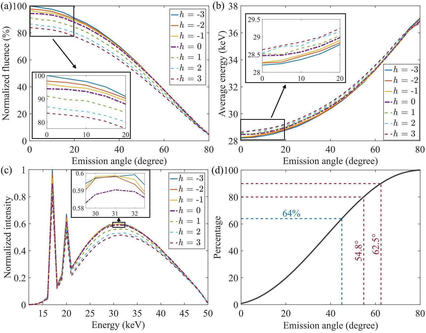
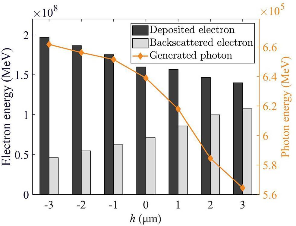
Figure 10 shows the energy-conversion results for the incident electrons in each case. As the value of h increases, the deposited electron and generated photon energies decrease, whereas the backscattered electron energy increases. These findings indicate that a recessed design can enhance the effectiveness of electron-stopping reactions in the anode and thus increase the X-ray fluence.
Effects of substrate material and thickness on X-ray filtering
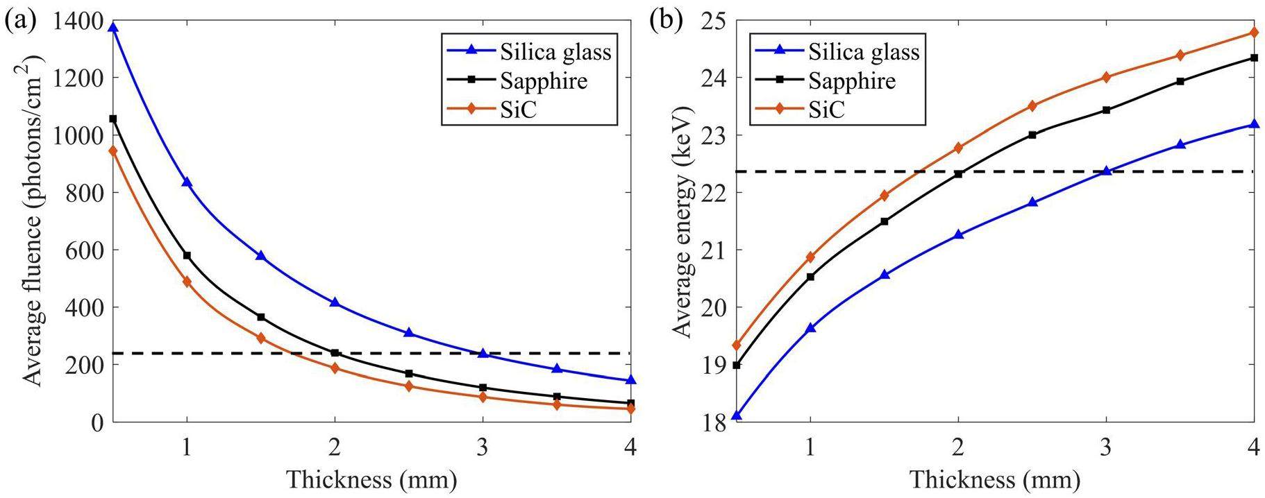
The average fluence and energy of the X-rays passing through silica glass, sapphire, and SiC ceramic substrates (with different thicknesses) are shown in Figs. 11(a) and 11(b). For a fixed thickness, silica glass yielded the lowest X-ray filtering effect because it had the highest average fluence and lowest average energy. As the substrate thickness increased, the average fluence decreased, whereas the average energy increased across all materials. The two dashed lines depict the average fluence and average photon energy for the 3 mm glass substrate, indicating that the filtering effect of X-rays by the 2 mm sapphire and 1.75 mm SiC ceramics is comparable to that of 3 mm silica glass.
Discussion
In this study, two detection modes in Geant4 were established to optimize and investigate the anode and substrate of the ZnO nanowire FPXS. Using the planar detection mode, the thickness of the microstriped array anode was optimized aim at higher X-ray fluences, and the variation in the X-ray spatial distribution was obtained as a function of the propagation distance. The characteristics of the X-rays generated from the microsemi-ellipsoidal anode at each emission angle were investigated using the hemispherical detection mode, and the reasons for the differences in the production of X-rays by the different microsemi-ellipsoidal structures were revealed by the energy conversion results of the incident electrons. The filtering effects of silica glass, sapphire, and SiC ceramic substrates on X-rays of different thicknesses were studied using the planar detection mode.
In the optimization of the microstriped array anode, the W target achieved a higher X-ray fluence than the Mo target at all acceleration voltages. Moreover, the optimal thickness of the W target was lower than that of the Mo target at all acceleration voltages, particularly at 90 kV, where the optimal thickness of the W target was only 1/5 of the Mo target. Therefore, the use of W as the anode material not only enhanced the X-ray fluence, but also reduced the aspect ratio of the anode strips, which may make device fabrication less challenging. The patterned distribution of X-rays on the rear side of the microstriped array anode disappeared at increasing propagation distances because the X-rays produced at each point of the anode were divergent. Nevertheless, in specific applications, such as grating-based X-ray phase-contrast imaging, where a structured X-ray distribution at the source is necessary, the microstriped array anode ZnO nanowire FPXS may have promising applications [20].
A microsemi-ellipsoidal anode with a recessed design improved the transmitted X-ray fluence, surpassing the film target by 5% and by approximately 16% than that of the raised design at small emission angles. Thus, a microsemi-ellipsoidal anode with a recessed design can be periodically employed in FPXS to enhance the X-ray fluence. The enhanced electron-stopping reaction within the anode with the recessed design allows more low-energy electrons to be involved in the production of X-rays, which may account for the decrease in the average energy of the X-rays. The considerable variation in the X-ray fluence and average energy at increasing emission angles can be explained by the filtering effect of the substrate, as X-rays with a large emission angle are associated with longer paths through the substrate; therefore, they have a lower fluence and higher average energy. It is important to note that Geant4 lacks the capability to simulate the trajectory of an electron in an electric field and can only assume a straight-line movement in vacuum.
In addition to filtering X-rays, the substrate supports the pressure difference caused by the internal vacuum and transfers heat from the anode to the surrounding environment. Diamond has been extensively used as a substrate material for transmission-type X-ray sources [36-38] because of its extremely high-mechanical strength, high-thermal conductivity, and low-X-ray absorption. However, challenges in large-area preparation have impeded their use in the ZnO nanowire FPXS. Among the candidate substrate materials, silica glass had the least prominent filtering effect on X-rays at a fixed thickness. However, considering the physical properties listed in Table 1, the use of sapphire as a substrate material can effectively reduce the attenuation of the X-ray fluence. In fact, sapphire with a thickness of 0.78 mm can achieve the same mechanical strength as 3 mm glass, given that the flexural strength is inversely proportional to the square of the thickness [39]. Consequently, the sapphire substrate exhibited the least prominent filtering effect on the X-rays and yielded the highest fluence at a fixed current. Moreover, when heat transport becomes a limiting factor for power enhancement in ZnO nanowire FPXS, the SiC ceramic presents a promising option owing to its high-thermal conductivity. The relationship between the substrate thermal conductivity and the maximum stable operating current of the ZnO nanowire FPXS is an issue for future research.
| Material | Flexural strength (MPa) | Elastic modulus (GPa) | Thermal conductivity (W/m/K) |
|---|---|---|---|
| Silica glass | 73 | 79 | 1.4 |
| Sapphire | 1035 | 435 | 40 |
| SiC ceramic | 550 | 410 | 120 |
Conclusion
The study utilized MC simulations to optimize the anode and substrate of the ZnO nanowire, cold cathode FPXS to enhance the X-ray fluence response. A microstriped tungsten anode array is beneficial for enhancing X-ray fluence. A microsemi-ellipsoidal anode with a recessed design can enhance the efficiency of electron-stopping reactions, thus increasing the transmitted X-ray fluence. Considering the filtering effect of X-rays and the physical properties of the substrate material, sapphire can effectively reduce the attenuation of the X-ray fluence. The simulated results can guide the fabrication and optimization of ZnO nanowire cold cathode FPXS in the future.
Methodology development and application of X-ray imaging beamline at SSRF
. Nucl. Sci. Tech. 31, 102 (2022). https://doi.org/10.1007/s41365-020-00805-7Review of current perspectives on low-energy X-ray intraoperative radiotherapy in early stage breast cancer
. Ther. Radio. Oncol. 3, 12 (2019). https://doi.org/10.21037/tro.2019.01.03Automated X-ray image analysis for cargo security: Critical review and future promise
. J. X-ray Sci. Technol. 25, 33-56 (2017). https://doi.org/10.3233/XST-160606An ultrahigh-resolution soft x-ray microscope for quantitative analysis of chemically heterogeneous nanomaterials
. Sci. Adv. 6,Addressable flat-panel x-ray sources for medical, security, and industrial applications
.X-ray tube thermal management
.Development ofgated carbon nanotube cold cathode for miniature X-ray source
.Achieving High Current Stability of Gated Carbon Nanotube Cold Cathode ElectronSource Using IGBT Modulation for X-ray Source Application
. Nanomaterials 12, 1882 (2022). https://doi.org/10.3390/nano12111882High-Performance Cold Cathode X-ray Tubes Using a Carbon Nanotube Field Electron Emitter
. Acs Nano. 16, 10231-10241 (2022). https://doi.org/10.1021/acsnano.2c02233Nanotube x-ray for cancer therapy: a compact microbeam radiation therapy system for brain tumor treatment
. Expert Rev Anticancer Ther. 14, 1411-1418 (2014) https://doi.org/10.1586/14737140.2014.978293An update on carbon nanotube-enabled X-ray sources for biomedical imaging
. Wiley Interdiscip. Rev. Nanomed. Nanobiotechnol. 10,Evaluation of carbon nanotube x‐ray source array for stationary head computed tomography
. Med. Phys. 48, 1089-1099 (2021). https://doi.org/10.1002/mp.14696Simulation on system configuration for stationary head CT using linear carbon nanotube x-ray source arrays
. J. Med. Imaging 8,Large-Scale Synthesis of Bicrystalline ZnO Nanowire Arrays by Thermal Oxidation of Zinc Film: Growth Mechanism and High-Performance Field Emission
. Cryst. Growth Des. 13, 2897-2905 (2013). https://doi.org/10.1021/cg400318fTransmission type flat-panel X-ray source using ZnO nanowire field emitters
. Appl. Phys. Lett. 107,Fully Vacuum-Sealed Diode-Structure Addressable ZnO Nanowire Cold Cathode Flat-Panel X-ray Source: Fabrication and Imaging Application
. Nanomaterials 11, 3115 (2021). https://doi.org/10.3390/nano11113115Flat-Panel Addressable Cold-Cathode X-Ray Source-Based Stationary CT Architecture
. IEEE Trans. Instrum. Meas. 72, 1-9 (2023). https://doi.org/10.1109/tim.2023.3271714Transparent Flat Panel X-Ray Source Using ITO Transmission Anode and ZnO Nanowire Cold Cathode
. IEEE Trans. Electron Devices 70, 3302-3307 (2023). https://doi.org/10.1109/ted.2023.3267757Beam and image experiment of beam deflection electron gun for distributed X-ray sources
. Nucl. Sci. Tech. 30, 1-12 (2019). https://doi.org/10.1007/s41365-019-0561-yFeasibility Study of a Cold-Cathode Flat-Panel X-Ray Source With Microarray Anode Target for Grating Interferometer Computed Tomography
. IEEE Trans. Nucl. Sci. 70, 2553-2560 (2023). https://doi.org/10.1109/tns.2023.3327904Design optimization of a periodic microstructured array anode for hard x-ray grating interferometry
. Phys. Med. Biol. 64,Design and numerical simulations of W-diamond transmission target for distributed x-ray sources
. Biomed. Phys. Eng. Express 5,Characteristics of miniature electronic brachytherapy x-ray sources based on TG-43U1 formalism using Monte Carlo simulation techniques
. Med. Phys. 39, 1971-1979 (2012). https://doi.org/10.1118/1.3693046A refined Monte Carlo code for low-energy electron emission from gold material irradiated with sub-keV electrons
. Nucl. Sci. Tech. 34, 54 (2023). https://doi.org/10.1007/s41365-023-01204-4Monte Carlo simulation of neutron sensitivity of microfission chamber in neutron flux measurement
. Nucl. Sci. Tech. 33, 78 (2022). https://doi.org/10.1007/s41365-022-01062-6Effect of Target Angle and Thickness on the Heel Effect and X-ray Intensity Characteristics for 70 kV X-ray Tube Target
. Prog. Med. Phys. 27, 272-276 (2016). https://doi.org/10.14316/pmp.2016.27.4.272Determination of Tungsten Target Parameters for Transmission X-ray Tube: A Simulation Study Using Geant4
. Nucl. Eng. Technol. 48, 795-798 (2016). https://doi.org/10.1016/j.net.2016.01.006Numerical optimization of transmission bremsstrahlung target for intense pulsed electron beam
. Nucl. Eng. Technol. 54, 666-673 (2022). https://doi.org/10.1016/j.net.2021.08.021Electron field emission Particle-In-Cell (PIC) coupled with MCNPX simulation of a CNT-based flat-panel x-ray source
.A Monte Carlo simulation study of a flat-panel X-ray source
. Appl. Radiat. Isot. 70, 1658-1666 (2012). https://doi.org/10.1016/j.apradiso.2012.04.011Tungsten Target Optimization for Photon Fluence Maximization of a Transmission-Type Flat-Panel X-Ray Source by Monte Carlo Simulation and Experimental Measurement
. IEEE Trans. Radiat. Plasma Med. Sci. 2, 452-458 (2018). https://doi.org/10.1109/trpms.2018.2849099Pulsed voltage driving enhanced electron emission in ZnO nanowire cold cathode flat-panel X-ray source
. Vacuum 199,Geant4—a simulation toolkit
. Nucl. Instru. Methods Phys. Res. B. 506, 250-303 (2003). https://doi.org/10.1016/s0168-9002(03)01368-8Validation of the Geant4 simulation of bremsstrahlung from thick targets below 3 MeV
. Nucl. Instrum. Methods Phys. Res. B 350, 41-48 (2015). https://doi.org/10.1016/j.nimb.2015.03.033Optimization of X-ray target parameters for a high-brightness microfocus X-ray tube
. Nucl. Instrum. Methods Phys. Res. B 264, 371-377 (2007). https://doi.org/10.1016/j.nimb.2007.09.023Design and demonstration of phase gratings for 2D single grating interferometer
. Opt. Express 23, 29399-29412 (2015). https://doi.org/10.1364/OE.23.029399Design and optimization of thin-film tungsten (W)-diamond target for multi-pixel X-ray sources
. Med. Phys. 49, 5363-5373 (2022). https://doi.org/10.1002/mp.15722High-resolution multicontrast tomography with an X-ray microarray anode-structured target source
. Proc. Natl. Acad. Sci. U.S.A. 118,The authors declare that they have no competing interests.

